|
|
|
|
|
|
6.5 Magnitude-Difference Bridges. Part 2.
|
12. The bridge as an analog computer. 13. Resistance bridges. 13a. Loading defect. |
13b. RVS resistance bridge. 13c. Tap compensation. 13d. Dual voltage sample. |
|
12: The bridge as an analog computer. An impedance, being a complex quantity, can be considered to posess two separate and distinct attributes; resistance and reactance. The same impedance, by taking its reciprocal, can also be considered as an admittance; with the separate attributes; conductance and susceptance. In both cases also, the two-dimensional nature of the quantity can be represented in terms of magnitude and phase. As was mentioned in the introduction (and discussed in detail in [Impedance Matching] ); if we can find a way of indicating the error in a particular impedance attribute in relation to some target value, and if we can do that for any attribute of our choosing; then there exist algorithmic solutions to the impedance matching problem that are guaranteed to terminate. In general, since null measurements of reactance, susceptance and phase are functionally indistinguishable (neglecting sign); this means that we can build automatic (or unambiguous manual) systems that can deal with any matching problem, provided that we can design bridges to measure magnitude, resistance, conductance and phase. The problem of how to design magnitude bridges has already been covered in the preceding sections. The design of phase bridges (to be discussed later) is also a fairly straightforward matter; and is related to the design of FM demodulators, phase-locking systems, and other well-known circuits. Hence, the principal area of difficulty is that of how to make the exotic bridges that measure resistance and conductance. The problem of how to make separate and automatic determinatons of individual impedance attributes is not comparable to that of manipulating the controls of a universal bridge and reading the quantity of interest from one of the dials. The reason is that we require bi-directional outputs, i.e., voltages suitable for driving galvanometers or servo amplifiers. The derived control voltages must also be free from contamination by the unwanted counterpart in each case, i.e., we need resistance measurements that are unaffected by reactance, and conductance measurements that are unaffected by susceptance. What we must do therefore, is devise schemes that cancel or eliminate the unwanted variable by combining the voltage and current sample outputs in a suitable way. This is a problem of analog computation, which we can solve by considering the nature of the analogs at our disposal. We can start by observing that a specific relationship exists between the sampling-network outputs. For a current-transformer bridge we can write: Vi = I Zi / N = V Zi / N Z Where I is the current in the transmission-line at the measuring point, V is the voltage across the line, and Z is the impedance seen when looking towards the load. In order to calibrate the bridge (and assuming that phase information needs to be conserved), we choose and adjust the components of the voltage sampling network so that, always, regardless of frequency: Vv = V Zi / N Z0 Where Z0 is the reference impedance, i.e.; the value of Z which makes Vi equal to Vv (here we generalise to the case where the reference impedance can, in principle, be complex; although in practice it is usually a resistance R0). Now notice that the phasor relationships above provide a complete determination of the impedance Z (at the chosen operating frequency); although it will take some further operations to separate-out the individual attributes (i.e., resistance and reactance, or magnitude and phase). The relationships also all contain the common factor Zi/N, which has nothing to do with the impedance information and is merely a property of the bridge. We only need to know Zi/N if we want to measure voltage and current. We do not need to know it for the purpose of characterising an impedance, because it can always be eliminated by taking a ratio. It is not only eliminated when we take the simple ratio of the sample outputs; it is also eliminated when we take the ratio of two arbitrary linear combinations (i.e., sums of multiples) of voltage and current samples because Zi/N can be removed from each sum as a common factor. This, as it will transpire, is the key to measuring a selected attribute of impedance, because we can always devise linear combinations that will cancel unwanted information. Zi/N has units of ohms. It is the common or mutual impedance shared as a constant of proportionality by the voltage and current samples. From this point of view, its function is to equalise the units of the sample measurements so that they are represented as voltages. Zi/N is also the transfer-impedance of the bridge, i.e., it is a scale-factor with dimensions of ohms that relates the current-sample output in volts, to the current input, in amps. In this sense, it is entirely analogous to the transfer-resistance (transresistance) of an amplifier that gives an output in volts for an input in amps; i.e., it is a gain-figure with dimensions of ohms. The quantity Zi/N is, specifically, the transfer-impedance (or 'transimpedance') of a current-transformer bridge. But we do not need to know the mechanics of the bridge in order to make use of its outputs. Hence we can generalise the concept of transimpedance to any bridge, regardless of the details, by assigning to it the symbol Zm (where 'm' stands for 'mutual'). This allows us to write generalised expressions for the voltage and current analogs: Vi = Zm I = Zm V / Z and Vv = Zm V / Z0 which are true for any bridge which gives Vv=Vi when Z=Z0. Thus if we know Zm, we can convert Vi into an absolute measure of current, and if we know Zm and Z0, we can convert Vv into an absolute measure of voltage. Note that it would be more convenient for those purposes if Zm were not complex. Conventional radio-frequency bridge networks do not form the basis for ideal ammeters and voltmeters; but that does not matter (in principle at least) when measuring ratios or looking for nulls. Although the sample outputs obtained from a bridge can be regarded simply as measurements of voltage and current, they can also be used as analogs of impedance, impedance ratio, or admittance, depending on how we consider them. This strangely co-operative behaviour stems from the fact that there exists a transconductance or a transresistance relationship between the output voltages (depending on which way you look at it), i.e., the bridge can exchange voltage for current or vice versa; and since voltage and current are related by Ohm's law (V/I=Z), this allows us to take reciprocals merely by swapping the output connections. To illustrate this point, observe firstly, from the relationships given above, that Vi is proportional to 1/Z and Vv is proportional to 1/Z0. Hence the outputs are analogs of admittance. Note however, that we can substitute IZ in place of V every time it occurs, so that: Vi = Zm I and Vv = Zm I Z / Z0 In this case, if we remove the common factor ZmI, then Vi represents unity (1+j0), and Vv represents the ratio Z/Z0, i.e., the bridge may be used to determine whether a ratio is greater than or less than 1. We may then also observe that Z0 is a system constant, and so if we use it to scale both samples we obtain: Z0 Vi = Zm I Z0 and Z0 Vv = Zm I Z In which case, if we remove the common factor Zm I, then Vi is proportional to Z0 and Vv is proportional to Z. These considerations enable us to construct the table of analogs shown below, where: Ym=1/Zm and Ym Zm = 1 . |
Table 12.1
|
|
|
|
|
|
|
|
|
|
|
|
|
|
|
|
|
|
|
|
|
|
|
|
|
|
To interpret the information given above, notice that the table
entries are obtained by multiplying the voltage at the head of
the table by the quantity in the left hand column. Thus we see:
that when Vi is taken to represent
admittance Y, then Vv represents
the reference admittance Y0; when
Vv is taken to represent impedance
Z, then Vi represents the
reference impedance Z0; and if
one of the sample voltages is taken to represent an impedance
ratio, the other represents unity. Note incidentally, that it
does not matter that the scaling factors contain either V
or I, which are phasor variables, because both sample
outputs are always affected equally by these quantities, and
the information we require is always in the relative magnitudes
and phases of the outputs. Also note that these straightforward
relationships arise because the component values of the sampling
networks have been chosen so that Vv
= Vi when Z = Z0. Had we chosen arbitrary networks, then it
would have been necessary to multiply one of the sample voltages
by a (complex) coefficient in order to obtain the relationships
shown. We already know that any impedance-related quantity can be obtained from bridge measurements, either directly or by a process involving some calculation. The calculations required moreover, always entail the operations of scaling (i.e., multiplication by a constant), addition (which includes subtraction, i.e., negative addition), reciprocation (i.e., inversion), and the taking of magnitudes. The foregoing argument now tells us that the business of taking reciprocals can be accomplished merely by swapping the sample outputs (giving a new slant on the idea that the bridge is a reciprocal network), and so we do not need to devise any special circuits for that purpose. We also have a perfectly good magnitude engine at our disposal in the form of the diode detector. This leaves us with only the so-called linear operations of scaling and addition; and since we are only interested in the relative magnitudes of the two samples, we can always arrange things so that the overall multiplication is by a number less than or equal to 1. Hence we can perform all of the required operations using ony passive components; those components being configured as potential dividers, summing networks and detectors. What we have to do now is work-out the required circuits. It is possible to deduce the general form for the sets of linear combinations needed to make bridges of any type by noting that it must encompass the balance conditions for the bridges we have already characterised. Observe therefore, that in all of the nulling-bridge circuits discussed so far, we have taken the voltage sample Vv and the current sample Vi and have subtracted them; either directly, or having first taken magnitudes. In the case of an ordinary impedance or reflected power bridge with a diode detector, the DC output of the system can be written: Vmeas = k |Vv - Vi| Where k is some detector function, determined by the properties of the detector and any losses due to loading effects (k varies with voltage, but since it affects both transfer functions equally, it cannot alter the balance condition). The balance condition is: |Vv - Vi| = 0 In the case of a magnitude bridge, the output is: Vmeas = k ( |Vv| - |Vi| ) and the balance condition is: |Vv| = |Vi| The set of linear combinations used in either case has the form:
Where, in the case of an impedance bridge, a suitable choice for the coefficients is a=1, b=-1, c=0 and d=0; and in the case of a magnitude bridge, a suitable choice for the coefficients is a=1, b=0, c=0 and d=1. Note however, that there are other choices due to the symmetry of the expression. Also, all of the coefficients can be multiplied by a common factor; although, to simplify the discussion, we will assume that a factor is removed so that the smallest non-zero coefficient always has a magnitude of 1. It is concievable that, in order to extract every attribute of an impedance, we might have to resort to schemes that involve adding and subtracting a string of magnitude brackets, each containing some multiple of Vv subtracted from some multiple of Vi (or vice versa - it makes no difference to a magnitude). Such complexity will prove to be unnecessary however; because all of the bridges we require can be built using two detectors; one to drive the DC output positive, and one to drive the DC output negative. That being the case, and recalling that only linear operations are required, equation (12.2) is the only non-redundant form for a general balance condition for all bridges. Hence the solutions we require will have the form of equation (12.2). Now knowing what the solutions will look like, we can narrow the range of possibilities considerably by noting that some choices for the coefficients produce no information, and that the pattern of coefficients required for a valid solution is highly restricted. This is not necessarily a good method for determining circuits, but it does prevent us from considering circuits that cannot work. In this document we take it as axiomatic that the sampling networks are designed so that Vv=Vi when Z=Z0. This means that the selected attribute will also match its target value when Z=Z0, and so a solution to equation (12.2) can only exist if the coefficients balance when Vv=Vi. Substituting Vv=Vi into (12.2) gives: | a Vi + b Vi | = | c Vi + d Vi | i.e: |Vi| | a + b | = |Vi| | c + d | This gives us the refined general balance condition:
Further restrictions are then obtained by noting that the solutions that produce no information, are: [ a=c, b=d ] and [ a=b=c=d=0 ]. There are still an infinite number of possible solutions; but if we ignore any that are simply multiples of other solutions, and if we start with coefficients of zero and work upwards, the search terminates rapidly. Each potential solution has to be proved of course, but it will transpire that the only values we will ever need for the coefficients are 0, ±1, ±2 and ±j. The unique solutions we require in order to build SWR, Match Meter and automatic impedance-matching bridges are summarised below: |
Table 12.4
|
|
|
|
|
|
|
|
|
|
|
|
|
|
|
|
|
|
|
|
|
|
|
|
|
|
|
|
|
|
|
The only point to remember in consulting this table is that the
quantities within any magnitude bracket can be multiplied by
-1 or ±j without affecting the outcome (because
rotational operations do not affect the magnitude of a vector).
Hence the solution for a phase bridge (for example) represents
several possibilities: | Vv + jVi | = | Vv - jVi | | -Vv - jVi | = | -Vv + jVi | | jVv - Vi | = | jVv + Vi | | -jVv + Vi | = |-jVv - Vi | etc. All of these provide the same information, but they suggest different ways of building the circuit. |
|
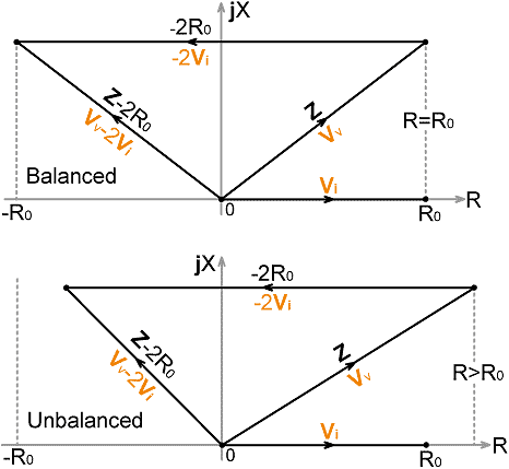
13. Resistance Bridges: When a reactance is placed in parallel with an impedance R+jX, the locus of the impedance (i.e., its point in the Z-plane) is moved around a circle of radius R/2, centred on the point R/2. Such a circle is known as a circle of constant conductance. When a reactance is placed in series with an impedance, the locus is moved along a line parallel to the jX axis, this line being called a line of constant resistance. An impedance matching process based on the adjustment of lumped reactances can be regarded as a set of Z-plane operations that serve to manipulate the load impedance onto the point R0+j0 by shifting it around circles of constant conductance and along lines of constant resistance. A resistance (R) bridge is a bridge that will remain balanced when an arbitrary (but not infinite) reactance is placed in series with the target load resistance. The utility of such a device lies in the fact that if a matching-network adjustment is performed to shift the load impedance onto the constant-resistance line corresponding to R=R0, the matching sequence can be completed by adjusting a series reactance. We can deduce the circuit for a resistance bridge by starting with the impedance analogs given in Table 12.1. Since resistance is the real part of impedance, we need to regard the voltage and current samples as impedance analogs. Vv must therefore be taken to represent Z, and Vi to represent R0 (strictly Z0, but here we will presume that X0=0). We then specify that the bridge must balance when R=R0, i.e., Z=R0+jX, regardless of the value of X. If we had an analog of jX, we could subtract it from Vv to obtain an analog of R, but all we have available is an analog of R0. Note however, that when the bridge is at balance: R0 +jX -2R0 = -R0 +jX This has the same magnitude as R0+jX, and so the solution to the problem is: | R +jX -2R0 | = | R +jX | i.e., | Z -2R0 | = | Z | when R=R0. which, when replaced by its analogs gives:
This is the balance equation for a resistance bridge; and of course, it has the form of the general balance condition (12.3) with coefficients [a=1, b=-2, c=±1, d=0]. The situation it represents, and the corollary: | Vv -2Vi | ≠ | Vv | when R≠R0 are illustrated in the impedance phasor diagrams below: |
|
Notice here also the directional information produced by the
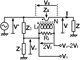
bridge: When R > R0 , |Z| > |Z -2R0| and |Vv| > |Vv -2Vi| Hence, if we connect the output of a detector producing a voltage proportional to |Vv| to the positive terminal of a centre-zero galvanometer, and the output of a detector producing a voltage proportional to |Vv -2Vi| to the negative terminal, then the meter will deflect in the positive direction when R > R0. The key to constructing a practical resistance bridge lies in synthesizing the vector Vv-2Vi. In order to do so accurately we need to preserve the relative phases of Vv and Vi, because any phase error will affect the magnitude of the resultant. Hence the frequency-response tracking considerations for the |Vv -2Vi| output are akin to those for an impedance bridge; i.e., we cannot use the magnitude-only approach discussed previously (although it could be used for the |Vv| output). A prototype circuit is shown below. This does not represent a general practical solution (its pitfalls and limitations will be discussed shortly), but it can be used to obtain the basic design equations. The most important point here is that, in order to obtain the voltage 2Vi, we simply define the output of the current transformer as 2Vi, and derive the voltage-sampling network so that: |
|
Vv = Vi
when Z = R0. i.e., having made the necessary definition, we proceed as though designing an ordinary impedance bridge. Hence, following previously established techniques, we have: 2Vi = I Zi / N = V Zi / (N Z) . . (13.1) where: Zi = Rik // jXLi |
 |
|
(Rik being the secondary load resistance
adjusted for losses). The output of the voltage sampling network
is: Vv = V' Z1 / (Z1 + Z2) . . . . . .(13.2) where V' = V + Vii = V + V Zii / Z = V [ 1 + Zi / (N² Z ) ] . . . . . .(13.3) Thus, when Z=R0: [ Z1 / (Z1 + Z2) ] [ 1 + Zi / (N² R0 ) ] = Zi / (2 N R0) . . . . . .(13.4) Which can be rearranged to give: |
|
|
Z1 |
|
|
Zi |
|
N |
|
|
|
This is the same as the balance condition for an ordinary impedance
bridge except for an extra factor of 2 on the right hand side.
We can now (in principle) choose suitable networks for Z1 and Z2 and
obtain expressions for the component values. Note however, that
although the design procedure is similar to that for an impedance
bridge, the resistance bridge still has the insertion defect
discussed in section 2. The reason is that Z does
not necessarily have to be equal to R0
when the bridge is balanced. Hence it is not strictly correct
to substitute R0 in place of Z
when establishing the relationship between V' and V.
As before however, the insertion defect error is usually small,
and vanishes when Z=R0. Separating the current-transformer secondary admittance into its real and imaginary parts and rearranging gives: |
|
Z1 |
|
Rik |
|
N |
|
jXLi |
Generic network solution (13.4b) |
| According to the procedure demonstrated earlier on several occasions, a voltage sampling network should now be chosen so that Z2/Z1 is separable into a frequency-independent real part, and an imaginary part that has a reciprocal frequency dependence. Before doing that however, it is necessary to be aware of a serious shortcoming of the basic circuit. |
|
13a. Loading defect: It is now that the complications and compromises begin. The problem is that the bridge must balance when the sampling networks are on load. This, of course, is the port-balancing problem introduced in section 4, but in a considerably less tractable form. |
| Shown on the right is the equivalent circuit of a resistance bridge loaded by two identical detectors each having an input resistance Rdet. Here the current-transformer is represented as an ideal transformer shunted by an impedance Zi=Rik//jXLi. It is assumed that the sampling network component values have been calculated using the method outlined above, but now the output voltages have been given primes to show that they have been modified by loading. |
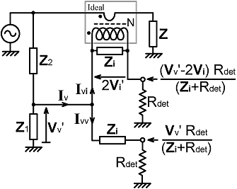 |
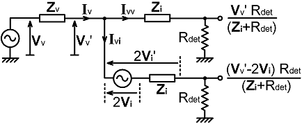
| Notice that a port-balancing network Zi has been placed in series with the "Vv" output. The reason is that the "Vv-2Vi" output is now effectively obtained via a potential divider consisting of the current-transformer output impedance (which is equal to Zi) and the detector input resistance. This causes the output to be multiplied by a factor Rdet/(Zi+Rdet). Hence, no analytical balance solution can exist unless the "Vv" output is also multiplied by the same factor, and this is accomplished by inclusion of the extra network. The point is most easily understood by considering the Thévenin equivalent circuit shown below: |
|
Here the voltage-sampling network is represented as a generator
that produces an unloaded voltage Vv
and has an output impedance Zv,
where: Zv = Z1 // Z2 Similarly, the current-sampling network is represented as a generator producing an unloaded voltage 2Vi, with an output impedance Zi. The port-balancing impedance modifies the "Vv" output to compensate for the difference between 2Vi and 2Vi'. Thus we have corrected for the finite output impedance of the current transformer; but we have not been able to do anything about the difference between Vv and Vv'. Vv' can be obtained from the voltage appearing across the VS-network output impedance, i.e.: Vv-Vv' = Iv Zv where, defining the currents according to the arrows in the diagrams: Iv = Ivv + Ivi The currents flowing towards the ports are: Ivv = Vv' / (Zi+Rdet) and Ivi = (Vv'-2Vi) / (Zi+Rdet) Hence: Iv = 2(Vv'-Vi) / (Zi+Rdet) and Vv-Vv' = 2(Vv'-Vi) Zv / (Zi+Rdet) . . . . . . (13.5) Notice here that both Iv and Vv-Vv' go to zero when Vv'=Vi. Also, at this point, Vv' →Vv, and so: Vv'=Vv when Vv=Vi This is an illuminating result because it tells us that, for the signal component at the generator frequency (i.e., treating the detector DC component separately), the voltage-sampling network becomes unloaded when the bridge is fully balanced, i,e, when Z=R0. The effect of the VS-network is to inject an unbalancing signal into the rest of the network, as can be understood by noting that the remaining network is inherently balanced if the VS network is removed. Hence the good news is that there is no need to modify the basic design equations when calculating component values. The bad news however (for this particular circuit) is that it is not possible to modify the basic equations to compensate for loading. Thus we discover that, even after port compensation, the prototype circuit has a flaw; which is that, although it balances perfectly when Z=R0, there will be an error in the balance point for R=R0 depending on the difference between Vv and Vi. This loading defect depends on the ratio: Zv/(Zi+Rdet), and so will be minimised when the VS network output impedance is small, or when the detector input resistance is large (or both). The former is difficult to achieve in instruments that are to be left in-line. The latter is not practical if the the circuit is required to drive a galvanometer directly, and (with certain types of VS network) Rdet may not even be sufficiently high if the detectors are designed to drive DC amplifiers. |
|
Quantifying the loading defect: The VS-network output impedance Zv will be substantially resistive in an RVS bridge, and substantially capacitive in a CVS bridge. Hence the consequences of the loading defect will be different for the two cases, and it becomes necessary to quantify the problem if we are to choose our networks sensibly. We start by rearranging equation (13.5) to separate Vv', as follows: Vv' = Vv - 2(Vv'-Vi) Zv / (Zi+Rdet) = Vv - Vv' [2 Zv / (Zi+Rdet) ] + Vi [2 Zv / (Zi+Rdet) ] Vv' [ 1 + 2 Zv / (Zi+Rdet) ] = Vv + Vi [2 Zv / (Zi+Rdet) ] Vv' [ 1 + 2 Zv / (Zi+Rdet) ] = Vv [ 1 + ( Vi / Vv ) 2 Zv / (Zi+Rdet) ] i.e.: |
|
|
|
1 + 2 Zv / (Zi+Rdet) |
|
|
|
From Table 12.1 we know that Vi/Vv is notionally
equal to R0/Z, but it is not exactly
so because of the insertion defect. Hence, for the sake of completeness,
we will derive it here in full. Equation (13.1)
gives us that: Vi = V Zi / (2 N Z) . . . . . .(13.7) Also equations (13.2) and (13.3) give us that: Vv = V [ 1 + Zi / (N² Z ) ] Z1 / (Z1 + Z2) but since Zv = Z1 // Z2 = Z1 Z2 / (Z1 + Z2) an alternative expression for the voltage sample is: Vv = V [ 1 + Zi / (N² Z ) ] Zv / Z2 . . . . . .(13.8) In establishing the general balance condition (13.4), we are required to choose the voltage sampling network so that: [ 1 + Zi / (N² R0 ) ] Zv / Z2 = Zi / (2 N R0) This allows us to substitute for Zv/Z2 in (13.8) above, so that we obtain: Vv = [ V Zi / (2 N R0) ] [ 1 + Zi / (N² Z ) ] / [ 1 + Zi / (N² R0 ) ] Hence, using (13.7): |
|
Vv |
|
V Zi 2 N Z [ 1 + Zi / (N² Z ) ] |
| i.e.: |
|
Vv |
|
Z + Zi / N² |
|
Z + Zii |
sample ratio |
| Where Zii is the current-transformer insertion impedance. Now, substituting this result into (13.6) we have: |
|
|
|
1 + 2 Zv / (Zi+Rdet) |
|
defect |
|
The information available here by direct inspection is that any
error in the sample ratio due to the finite insertion impedance
will make a contribution to the loading defect. The nature of
that contribution depends on Z moreover; and since Z
is a random variable, it is not possible to engineer the insertion
defect with a view to minimising the loading defect. Having made
that point however, we should note that if the initial design
work has been done properly, Zii
should be very small in comparison to R0.
Hence it will help us to focus on more important issues if we
use the approximation Vi/Vv=R0/Z from now
on. Now we will make the substitution that causes this perplexing problem to unravel. Referring again to Table 12.1, we note that in using the sample voltages as impedance analogs, Vv represents and is proportional to Z. Hence we can put the loading defect into the form: |
|
|
|
1 + 2 Zv / (Zi+Rdet) |
|
| Where Z' is the impedance which appears to be connected to the bridge. Multiplying Z into the bracket gives: |
|
|
1 + 2 Zv / (Zi+Rdet) |
|
Now recall that the design objective is to create a bridge that
balances when Z=R0+jX, regardless
of X. We already know that the balance error disappears when
X=0, and it follows that it will be most serious when |X| is
large. We will now develop a simple formula that will enable
us to evaluate this problem. Firstly, to minimise clutter, we will assign the symbol kv to the ratio 2Zv/(Zi+Rdet). Hence: |
|
|
1 + kv |
|
We can also develop an idea of the magnitude of kv by considering some typical starting-points
for bridge design. Firstly (assuming that the target load resistance
is 50 Ω) about the worst case for Zv
occurs when we must design a sensitive circuit for permanent
monitoring of (say) a 100 W radio transmitter. In that case, since we need to obtain port outputs of several volts without abstracting a significant amount of power, |Zv| can be as much as 500 Ω. Secondly, if the detectors must drive a 50-0-50 μA meter in opposition, they will have to have a fairly low value of load resistance, say 10 kΩ, so that they can sink current as well as source it. Hence the detector input resistance Rdet will be about 5 kΩ. The current-transformer output impedance Zi will always be small relative to Rdet, and so |kv| will be about 0.2 for a sensitive bridge driving a galvanometer directly. If we are allowed the luxury of some amplifiers, then the detector loads can be 100 kΩ or more, in which case Rdet can be greater than 50 kΩ and we reduce |kv| to 0.02 or less. Hence it is useful to bear in mind is that |kv| will be somewhere in the region of 0.2 to 0.02. Now let us define the load impedance at balance as: Zbal = R0+jX thus: |
|
|
1 + kv |
| Where the real part of Z'bal (R'bal say) corresponds to the point at which the bridge will actually balance. A little rearrangement gives: |
|
|
1 + kv |
where kv = 2 Zv / (Zi+Rdet) |
|
|
This expression tells us immediately that the bridge will balance
perfectly if kv is real. If there
is any imaginary component in kv
however, it will produce an additional real term when the load
reactance term is rearranged. Since X can take on any value,
and it is not unusual to encounter reactances between -2500 and
+500Ω when evaluating antennas prior to matching, the error
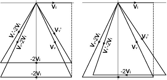
is potentially very serious. Say, for example, that we design a 50 Ω bridge with a resistive voltage-sampling network, but try to correct for the falling secondary reactance of the current transformer at low frequencies by placing a coil across the lower voltage-sampling arm. Then, to keep things simple by using a 3-4-5 triangle, we might have Zv=400+j300 at 1.9 MHz, giving kv=0.16+j0.12 when |kv|=0.2. Operating at 1.9 MHz we are likely to encounter electrically-short antennas, and so let us see what happens when X=-2500Ω. Z'bal = 50 - j2500 / ( 1.16 + j0.12 ) Multiplying the numerator and denominator of the reactance term by the complex conjugate of the denominator gives: Z'bal = 50 - j2500 ( 1.16 - j0.12 ) / ( 1.16² + 0.12² ) = 50 + ( -300 - j2900 ) / 1.36 = -170.6 - j2132 R'bal = -170.6 Ω Because R'bal is negative in this case, the bridge is not so much inaccurate, as incapable of balancing when the load has a large negative reactance. Now let us see what happens if we try to use a capacitive VS network. In that case, ignoring any LF compensation, we might have kv= -j0.2 at low frequencies. Thus: Z'bal = 50 - j2500 / ( 1 - j0.2 ) = 50 - j2500 ( 1 + j0.2 ) / ( 1 + 0.2² ) = 50 + ( 500 - j2500 ) / 1.04 = 530.8 - j2404 R'bal = 530.8 Ω Again the error is preposterous, and we are forced to conclude that the prototype circuit is only workable if we use an un-compensated resistive VS network. It will not even be possible to use a trimmer capacitor to balance the capacitance in the two arms. Even if Zv is purely resistive, the potential for error is so great that it is advisable to check the effect of the tiny reactive component that can be introduced into kv by Zi. Say, for example, that the current transformer is loaded with 50 Ω and we decide to make the secondary parallel reactance 7 times greater than the load resistance at 1.8 MHz. Hence we have XLi=+350Ω and Zi = 50 // j350 = j17500 / (50 + j350) = j17500 (50 - j350) / (50² + 350²) =(6125000 + j875000) / 125000 Zi = 49 + j7 Ω Now, ignoring the resistive component, which is trivial in comparison to Rdet, we have: kv = 1000 / (5000 + j7) = 1000 (5000 - j7) / (5000² + 7²) which, to as good an approximation as is worth the bother gives: kv = 0.2 - j0.00028 Now, if X is -2500Ω, we have: Z'bal = 50 - j2500 / ( 1.2 - j0.00028 ) = 50 - j2500 ( 1.2 + j0.00028 ) / ( 1.2² ) R'bal = 50.5 Ω In this case, the error is only 1%, which is perfectly acceptable in impedance matching applications; but this example relates to a transformer with a large secondary inductance, and we will run into trouble at high frequencies unless the length of the winding wire is kept short, i.e., the transformer core material will need to be of very high permeability. The way in which the loading defect affects the balance condition is illustrated in the two phasor diagrams below, which give the relationships between Vi, Vv and Vv' when the load reactance is negative. |
|
In the left-hand diagram, kv is
real and so, when the ports are loaded, the locus of Vv (i.e., the point at the end of the line representing
Vv) is shifted along a line which
corresponds to a line of constant resistance in the Z-plane.
The change in the magnitude of Vv
may be considerable, but the condition |Vv'-2Vi|=|Vv'| when
R=R0 is always maintained, and so the
nulling condition is unaffected. In the right-hand diagram, kv is taken to be purely imaginary (such as if we were to try building a CVS version of the bridge). In this case, port loading moves the locus of Vv diagonally, but mostly in the resistance (horizontal) direction of the corresponding Z-plane. Now |Vv'-2Vi| is not equal to |Vv'| when R=R0, and the bridge is defective. The seriousness of the problem, as illustrated by the numerical examples given earlier, can be much worse than the diagram suggests. |
|
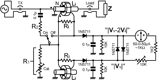
13b. Practical RVS resistance bridge: From the foregoing discussion, it is evidently not practical to use a reactive voltage-sampling network when realising a resistance bridge from the basic circuit topology. It is not even practical to correct for the falling frequency-response of the current transformer at low frequencies. Even if we import DC power for amplifiers with a view to raising the detector input resistances, it is still unlikely that acceptable broadband performance can be achieved unless the voltage-sampling network output impedance is as close to perfectly resistive as is possible. This leads us to two observations: firstly, that the VS network will have to absorb a significant amount of power; and secondly, that the current-transformer will need to have a large secondary inductance. In the latter case also, it is best not to obtain that inductance by using a large number of turns, since to do so will run us into difficulties at high frequencies. Hence the inductance must come from the use of high-permeability core material. All of this leads to the conclusion that the basic circuit is not a good starting point for the design of precision bridges, and it is not suitable for bridges to be used in conjunction with high-power radio transmitters. Having noted the caveats however; there is still, in the practice of antenna characterisation and matching, an application for simple instruments of moderate accuracy (a few %) capable of withstanding a maximum power throughput of, say, 100W. We may not be able to achieve the very low power abstraction (< 1%) typical of CVS bridges; but 3% is feasible, and is acceptable in circuits that are not intended to be left permanently in-line. There are, of course, general design as well as theoretical issues to be considered when developing a practical bridge. We can address such matters, and exercise the equations given earlier, by means of a worked example. For that purpose, the circuit diagram below shows a resistance bridge with some of the details filled-in, and some yet to be decided. We will assume the following requirements: that the bridge will balance when the resistive component of the load impedance is 50 Ω; that it will operate with reasonable accuracy from 1.6 to at least 30 MHz, that it will not be damaged when the transmitter is delivering 100 W continuously into a matched load; and that it will give good sensitivity with the voltages and currents associated with load power of around 10 W. |
|
Notice firstly, that a DC blocking capacitor has been placed
in series with the upper voltage-sampling arm (R2).
This component has been included, not because the presence or
absence of a DC path to ground through the generator and load
will affect the detector response (which it will to a small extent),
but because there might be DC signals on the line for actuators
or telemetry. Any direct voltage (positive or negative) applied
via the VS network will reduce the detector RF sensitivity. A
0.1μF ceramic disk capacitor provides immunity in this respect,
but it will need to be rated to withstand about 100 V RMS. The
reactance of a non-inductive 0.1 μF capacitor at 1.8 MHz is
-0.88Ω , which is negligible in terms of its contribution
to the network output impedance. The bridge has been provided with an on-off switch. There are numerous ways in which this can be done, but the main point is to recognise that the device can be "removed from the line" in ways other than messing around with plugs. In this case we disconnect the upper VS arm and short-out the current transformer secondary, the latter operation reducing the insertion impedance effectively to zero. The use of a switch having a low capacitance to ground (such as a Yaxley wafer) is advised. Notice that this method will only work if the transformer has a Faraday shield. If there is no shield, the through-line will be capacitively coupled to the detector inputs, and slightly unequal DC outputs may be produced at high frequencies. The meter response has been made quasi-logarithmic by means of a pair of shunt diodes [see section 9a]. This eliminates the user sensitivity control, but also compensates for an undesirable property of this particular circuit. The issue is that both detectors share the same DC port resistance. When the bridge goes out of balance, the detector giving the largest output will tend to bias its opponent out of conduction. When that happens, the dominant detector will annex all of the port resistance to itself, thereby undergoing an increase in gain. In the absence of limiter diodes, there will be an evil tendency for the meter to slam from end-stop to end-stop as as the load impedance is swept across the balance point. As mentioned previously, due to high sensitivity around the nulling point, good port balancing is required when using a logarithmic meter. The port-balancing inductor is simply a replica of the current-transformer with nothing connected to the primary (but the shield is earthed to maintain symmetry). So now to the RF part of the design. We start by observing that we will need a fairly large voltage from the current-transformer because the output is effectively shared between the two detectors when the bridge is at full (Z=R0) balance. We cannot make it too large however, because the insertion impedance will then become excessive. Limiting the mid-band insertion resistance to about 1% of R0 is a fairly good idea, and since Rii=Ri/N², this means that if we load the transformer with a 50 Ω resistance, the secondary winding should have no less than 10 turns. A 100 W transmitter driving a 50 Ω load is producing an output or 70.7 V and 1.41 A RMS. A typical protected push-pull (Granberg type) power amplifier can be expected to deliver at most, either the full current, or the full voltage, but not both, if the load is a serious mismatch. Hence we expect a maximum load current of 1.41 A. A 10 turn current-transformer with a 50 Ω secondary load will produce a midband output of |I|Ri/N= 7.07 V (neglecting losses) when the transmitter is giving its full output current, and if the mismatch is so bad that the line voltage is nearly zero, most of this will be applied to the "|Vv-2Vi|" detector. The 1N5711 Schottky diode can withstand a peak-inverse voltage of 70 V, whereas the greatest PIV encountered will be about 7.07×2×√2=20 V. Hence we have a large detector safety margin, but it will not be so good if germanium diodes are used as substitutes. When the matching sequence is nearing completion, the current-transformer output will be split about equally between the two detectors. We might expect the transmitter drive level to be set for an output of between 1 W and 10 W while matching adjustments are in progress, and so we need usable sensitivity for load currents of between √(1/50)=0.14 A and √(10/50)=0.45A. These correspond to detector drive voltages of between 0.35 V and 2.24 V. The detectors will still work (just about) with 0.35 V AC input, and we only need a difference of about 50 mV between the two DC outputs in order to obtain a fair meter deflection. Hence the bridge will still be usable when the transmitter is set to deliver 1 W. Now however, we have the problem that LF compensation is not possible. This means that the transformer secondary inductance must be at least 7 times the secondary load resistance, i.e., we need XLi >350 Ω at (say) 1.8 MHz, which corresponds to an inductance of >31 μH. A little trawling of transformer-core catalogues is called for (or see data tables in [current transformers] ), and it transpires that the Amidon FT50-43 bead is suitable (and fits nicely over a stub of 5 mm diameter PTFE coaxial cable). The bead has an AL of 523 nH/turn² (nominal, ±25%) and so (for N=10) gives 52 μH in the centre of the tolerance range, and 39 μH in the worst case. The transformer looks good, and so now we can calculate the power rating of the secondary load resistor(s). With 100 W line throughput, we will have 7.07 V across the secondary terminals and hence 7.07²/50 = 1 W dissipated. The transformer load can be two 0.6 W 100 Ω resistors in parallel. Using a pair of resistors helps to offset the unnecessarily high inductance of helically-cut metal-film resistors. Carbon-film resistors might even be used here, although they are not so stable. We need the voltage-sampling network to be of low reactance. This means that the resistors need to be of sufficiently low value to swamp the parallel capacitance. Hence the choice is a compromise between power dissipation and high-frequency balance error. There are no hard-and-fast rules to apply in deciding the resistance of the series combination (R1+R2), it depends on the design of the resistors; but a total dissipation of about 2 W for 70.7 V at the generator is a reasonable starting point. This is somewhat greater than required for a bridge that can have compensation networks, but then again, we have provided an on-off switch. Thus we have R1+R2 = 70.7²/2 = 2500 Ω; or thereabouts, depending on available preferred values. Now we apply equation (13.4b), but drop the term containing the transformer secondary susceptance on the grounds that there is nothing we can do about it anyway. Thus: |
|
R1 |
|
Ri |
|
N |
|
|
|
So: R2 / R1 = 20 +0.2 -1 = 19.2 R2 = 19.2 R1 R1 + R2 = 2500 R1 + 19.2R1 = 2500 R1 = 2500 / 20.2 = 123.76 Ω R2 = 2376.2 Ω This is an awkward value, and so we will change it to 2.4 kΩ, allowing the use of two 1.2 k 1 W resistors in series for the upper arm. Now we get: R1 = 2400/19.2 = 125 Ω which can be made up as a 100 Ω resistor in series with a 50 Ω multi-turn cermet pot (e.g., Vishay type 43p). The large adjustment latitude makes it unneccessary to use resistors of high initial tolerance elswhere in the sampling networks. The detectors however need to be well balanced, and so resistors of (at worst) 1% tolerance should be used for the detector loads. On the DC side however, inductance is irrelevant, and so helical metal-film resistors can be used with impunity. |
|
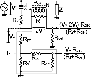
13c. Tap compensation: Production engineers, and other practitioners of the dark arts, will want to delete the port balancing network. As mentioned earlier however; there is no exact solution for the balance condition when that is done, and the best that can be achieved is an "almost but not quite" resistance bridge. The consequence moreover will be a permanent systematic error; as opposed to the insertion and loading defect errors, which at least have the decency to disappear when Z=R0. Still, it has to be said that, if the current-transformer output impedance (which is not far-off resistive when XLi is large) is less than 2% of the detector input resistance, the error might be deemed acceptable. We cannot go on making compromises indefinitely however, because the cumulation will eventually become too great. We are really only allowed about 10% balance error before the bridge is classified as useless, and <5% (1.1 SWR) is a sensible target. We might seem to be comfortably within that limit; but there are less controllable issues such as the Faraday-shield capacitance and component parasitics, which might direct us not to take further liberties. There is however, a partial port-balancing solution that requires only two resistors in principle, and only one resistor in practice. This involves taking the "Vv" output from a tap in the voltage-sampling network, slightly below the point to which the current-transformer is connected. Recall that the "Vv-2Vi" output is multiplied by a factor Rdet/(Zi+Rdet) due to the finite output impedance of the current-transformer. Here we must assume that XLi is large, and so we can write this factor as Rdet/(Ri+Rdet). By tapping at the appropriate point, we can arrange things so that the "Vv" output is also multiplied by Rdet/(Ri+Rdet). The limitation of the method is that Rdet varies with drive level [see: Diode det for RF meas]; but it settles down once the drive reaches about 1.5 V RMS, and so we can achieve near-perfect precision (mid band at least) when the transmitter power is turned-up at the end of the matching sequence. |
| The circuit is shown on the right. Here we define Vv as the voltage to be summed with the current sample, whereas the direct "Vv" output is taken from a tap on the other side of a port compensation resistance Rpc. Note that another resistance of value Rpc has been placed in series with the detector input, its purpose being to ensure that the DC resistance looking back into either of the ports is the same. Whether this DC port-balancing resistance is actually included will depend on how large Rpc is in comparison to the tolerance-related uncertainty in Rdet (and unless there is something horribly wrong with the design, it will be small). |
 |
|
We can solve for the network component
values in two stages. We start by lumping everything connected
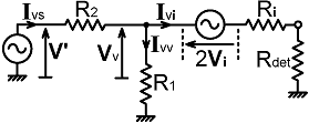
to the lower voltage sampling arm into a single resistance R1. Hence, by inspection: R1 = Rpc + R1' // (Rpc + Rdet) . . . . . . (13.11) A value can be placed on R1 once we have chosen R2, as was done in the example in the preceding section; but this time we need to calculate the ratio R2/R1 with an allowance for the loading caused by the detector connected to the "Vv-2Vi" port. To do that, we can use the Thévenin equivalent circuit shown below. The current flowing from the generator into the VS network is: Ivs = (V' - Vv) / R2 |
|
The current flowing through the detector is: Ivi = (Vv - 2Vi) / (Ri + Rdet) and the current flowing through R1 is: Ivv = Vv / R1 Hence: |
 |
|
R2 |
|
Ri + Rdet |
|
R1 |
| Which, upon moving all instances of Vv to the left hand side, gives: |
|
|
|
R1 |
|
R2 |
|
Ri + Rdet |
|
|
R2 |
|
Ri + Rdet |
|
Now we can substitute for all of the voltages to obtain a common
voltage factor V (the voltage across the load) on both
sides. From equation (13.3),
bearing in mind that XLi is assumed to
be large: V' = V [ 1 + Ri / (N² Z ) ] and from equation (13.1) 2Vi = V Ri / (N Z) Hence: |
|
|
|
R1 |
|
R2 |
|
Ri + Rdet |
|
= V |
|
|
1 + |
N² Z |
|
R2 |
|
N Z (Ri + Rdet) |
|
|
The relationship between Vv and
Vi is, of course, determined by
the full balance condition; i.e.: when Z → R0 , Vv → Vi → V Ri / (2N R0) Thus, substituting for Vv, cancelling V from both sides, and changing all instances of Z to R0, we get: |
|
2N R0 |
|
R1 |
|
R2 |
|
Ri + Rdet |
|
|
|
|
N² R0 |
|
R2 |
|
N R0 (Ri + Rdet) |
| Multiplying both sides by 2NR0/Ri gives: |
|
R1 |
|
R2 |
|
Ri + Rdet |
|
R2 |
|
Ri |
|
N |
|
|
Ri + Rdet |
| Multiplying both sides by R2 and subtracting 1 then gives: |
|
R1 |
|
Ri |
|
N |
|
Ri + Rdet |
|
| On comparing this with equation (13.10), it will be seen that the loading associated with the "Vv-2Vi" port introduces a term R2/(Ri+Rdet) into the voltage-sampling resistance ratio. Notice that this term is positive, i.e., the current 'drawn' from the network mandates either an increase in R2 or a reduction in R1 in order to correct for it. The reason is that 2Vi is twice as great as Vv when the bridge is fully balanced (and the two sample voltages are in phase). Hence, the 'loading' amounts to an injection of current, which gives rise to a tendency for Vv to increase. In view of that, we might have pointed the Ivi arrow in the opposite direction when making the initial definitions; but the definition is irrelevant provided that the resulting sign convention is followed correctly. |
| Now, having an expression that will allow us to determine R1, it remains for us to determine Rpc and R1'. We will need to solve two simultaneous equations in order to do that. One of those has been given already as (13.11). The other can be deduced from the Thévenin equivalent circuit shown on the right. |

|
|
We start by writing expressions
for the voltages Vv" and Vv', this being a simple potential-divider problem: Vv" = Vv [ R1' // (Rpc + Rdet) ] / [ Rpc + R1' // (Rpc + Rdet) ] but, equation (13.11) gives us that: R1 = Rpc + R1' // (Rpc + Rdet) Hence: Vv" = Vv [ R1' // (Rpc + Rdet) ] / R1 T he port voltage, relative to Vv" is: Vv' = Vv" [ Rdet / (Rpc + Rdet) ] and substituting for Vv" gives: Vv' = Vv [ R1' // (Rpc + Rdet) ] Rdet / [ R1 (Rpc + Rdet) ] In order to effect the port compensation, we define Vv' as: Vv' = Vv Rdet / (Ri + Rdet) Hence: Rdet / (Ri + Rdet) = [ R1' // (Rpc + Rdet) ] Rdet / [ R1 (Rpc + Rdet) ] Which, upon expanding the parallel product comes out as: |
|
Ri + Rdet |
|
(R1' + Rpc + Rdet) |
R1 (Rpc + Rdet) |
|
This can easily be solved for R1' as follows: R1' (Ri + Rdet) = R1 (R1' + Rpc + Rdet) R1' (Ri + Rdet - R1) = R1 (Rpc + Rdet) Hence: R1' = R1 (Rpc + Rdet) / (Ri + Rdet - R1) . . . . . . . . . . . (13.13) We will use this expression to eliminate R1' from equation (13.11). Writing (13.11) with the parallel product expanded gives: R1 - Rpc = R1' (Rpc + Rdet) / (R1' + Rpc + Rdet) This can be rearranged to separate R1' as follows: (R1' + Rpc + Rdet) / R1' = (Rpc + Rdet) / (R1 - Rpc) (Rpc + Rdet) / R1' = [(Rpc + Rdet) / (R1 - Rpc)] - 1 Hence: |
|
R1' |
|
(R1 - Rpc) |
|
(Rpc + Rdet) |
| Putting the right-hand-side on a common denominator gives: |
|
R1' |
|
(R1 - Rpc) (Rpc + Rdet) |
|
(R1 - Rpc) (Rpc + Rdet) |
| and substituting for 1/R1' using (13.13) gives an expression containing only Rpc and supplied parameters: |
|
R1 (Rpc + Rdet) |
|
(R1 - Rpc) (Rpc + Rdet) |
|
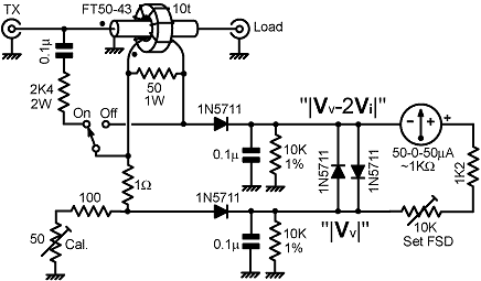
We can solve for Rpc as follows: ( Ri + Rdet - R1 ) ( R1 - Rpc ) = R1 ( 2Rpc + Rdet - R1 ) R1 ( Ri + Rdet - R1 ) - Rpc ( Ri + Rdet - R1 ) = R1 ( 2Rpc + Rdet - R1 ) R1 Ri - Rpc ( Ri + Rdet - R1 ) = 2 R1 Rpc R1 Ri = Rpc ( Ri + Rdet + R1) Hence: Rpc = R1 Ri / ( Ri + Rdet + R1) . . . . . . . . . . . (13.14) It is possible, in principle, to determine Rdet and R1 very accurately by a process of iteration, but there is little point in doing so. Firstly, Rdet varies with drive level; and secondly, Rpc, which is the main quantity of interest, will turn out to be a very small resistance; which means that it will take a sizeable variation in Rdet to cause us to switch from one preferred value to the next. Hence, all we need is a reasonable estimate for Rdet. Recall, from [Diode det], that the limiting value of Rdet (for impractically high input voltages) is given by: Rdet = (Rport + Rds + Rd) / 2 Where Rds is the diode internal resistance (about 25 Ω for a 1N5711) and Rd is the detector load resistance. Rport is the apparent DC resistance looking back into the port; and in this case we must note that the actual resistance is shared by two detectors. When the bridge is balanced, the detectors will be giving equal outputs, which means that the DC voltage drop across the shared resistance will be exactly twice the voltage produced by a single detector. We can allow for that by doubling the shared resistance. Hence, for the tap-compensated resistance bridge, the limiting value for the detector input resistance is: Rdet = (2R1' + Rpc + Rds + Rd) / 2 The actual input resistance at balance will be a few % higher than this. In the example given at the end of the previous section, we chose R2=2.4 kΩ and obtained R1=125 Ω. If we leave all of the other design choices alone, 2R1 from that calculation is a fair estimate for Rport, and so the limiting value for Rdet will be about (250+25+10 k)/2 = 5138 Ω. The detector is modelled on this basis in the spreadsheet R_det_Rin.ods, using the method described in [Dioded det], and it is found that Rdet varies between about 5730 and 5512Ω for drive levels between 2.2 V and 3.5 V RMS (corresponding to between 10 W and 100 W delivered to a matched load). Hence we will use a compromise value of 5620 Ω for further calculations. For R0=50 Ω, R2=2.4 kΩ, N=10, and Ri=50 Ω, equation (13.12) gives: R2 / R1 = 20 + 0.2 - 1 + 2400 / (50 + 5620) = 19.623 Hence: R1 = 2400 / 19.623 = 122.3 Ω Equation (13.14) gives: Rpc = 122.3 × 50 / (50 + 5620 + 122.3) = 1.06 Ω Finally, for completeness, using equation (13.13): R1' = 122.3 (1.06 + 5620) / (50 + 5620 - 122.3) = 123.9Ω We end up with the circuit shown below: |
|
Notice that the resistor in series with the input to the "|Vv|" detector has been omitted. The reason
is that the tolerance of the detector load resistor gives rise
to an uncertainty of about 50 times Rpc
in the detector input resistance, and so there is no point in
including it. The smallness of Rpc, of course, begs the question: "is there any point in tapping into the VS network for such a small correction?" The answer however is yes, the reason being that the detectors can produce outputs of several volts, and it only takes a difference of a few millivolts to produce a visible meter deflection. The popularity of CLC T-networks implies that the bridge is likely to be used in situations in which a variable capacitor of low ESR is presented in series with an otherwise resistive load. The port-compensation resistor reduces the tendency for the balance point to change as the series reactance is adjusted. |
|
13d. Dual voltage-sample (precision) resistance bridge: In view of the theoretical complexities involved in persuading the prototype resistance bridge to produce acceptable (but unimpressive) performance; in may come as welcome relief to discover that there is a resistance bridge circuit that has no loading defect, places no restrictions on the choice of voltage-sampling network, and requires no complicated mathematical proofs in order to determine its properties. The downside is an increased component count, and a relatively complicated calibration procedure; but there is no difficulty in designing bridges for use in conjunction with kilowatt transmitters, and the insertion defect is the only significant limitation on the ultimately achievable precision.. |
| The circuit in its generic form is shown on the right. The only difference between it and the basic circuit described earlier is that there are now two identical voltage sampling networks (and the attendant problem of how to make them identical). The generic balance solution is the sames as that for the unloaded shared-VS bridge (13.4b), but now detector loading has no effect on the balance condition; which means that the choice of VS networks is at the circuit-designer's discretion. |
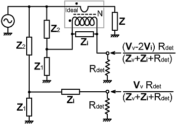 |
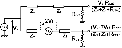
| If we design the dual-VS bridge so that the sampling networks give the outputs Vv and 2Vi when unloaded, the actual port voltages are as shown in the diagram above (where: Zv=Z1//Z2). The reason why those are the voltages obtained should be obvious by inspection of the Thévenin equivalent, which is given below: |
|
If the detectors are substantially identical, and a port-balancing
impedance is placed in series with the "Vv"
output; then both outputs are multiplied by the common factor
Rdet/(Zv+Zi+Rdet), which after
rectification comes out as Rdet/|Zv+Zi+Rdet|.
If |Zv| should be relatively large
at some frequencies (as it tends to be with CVS networks), the
bridge might become insensitive; but the balance point is completely
immune to detector loading provided that both detectors present
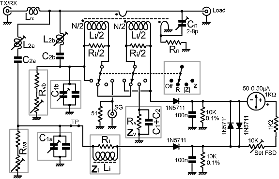
the same input resistance for the same drive level. A possible implementation is shown below. In this case (for the sake of discussion at least), adjustments and compensation networks have been included with a view to achieving the best possible performance. A rotary switch also makes available all of the functionality for which theory has been presented so far; although the principal reason for including it is that network reconfiguration is required during calibration. |
|
The main current-transformer secondary winding has been split
into two parts, both of which produce the voltage Vi when unloaded. These should be capacitively
isolated (i.e., definitely not bifilar). They are placed
in series to provide 2Vi for the
resistance bridge "R" mode. Note that if the secondary
load resistors are excessively inductive, the effective secondary
parallel capacitance (Ci) will be negative,
and this will cause a problem with neutralisation. [see Eval
& opt, section 13] If helically-cut metal film resistors
are used, connecting them in parallel pairs is usually sufficient
to obtain a positive value for Ci. The
resistor lead lengths should, of course, be kept to the absolute
minimum. Generally, designs start with a trial value for Ri of 50 Ω, and usually end there. Hence
each instance of Ri/2 might be realised
as (say) two 49.9 Ω 0.1% 0.6W MF resistors in parallel. The inductance of half of the secondary winding is marked as Li/2, not Li/4 as might be calculated from the core AL. This is not a mistake. When both windings are loaded equally, mutual inductance causes the effective inductance of each winding to be doubled. Switching the bridge off is effected by shorting-out the transformer secondaries only. The voltage-sampling networks remain connected. This is permissable because the power-consumption of the LF compensation resistances Rva and Rvb is trivial. It is also necessary, because the power-factor correction inductance Lα is calculated to compensate for any excess through-line capacitance (see section 6), and if the VS networks are removed the supplementary inductance will be incorrect. An impedance magnitude "|Z|" mode is included because it can be had for the cost of a port-compensation network Zv. A fixed 1% carbon-film resistor, of the preferred value nearest to the measured value of Rva after calibration, is probably adequate for this network. When the switch is in the position "Z" the instrument becomes a precision impedance bridge with its Vv-Vi port connected to a socket marked "SG" (signal generator). With a transceiver set to 'receive' connected to the "TX/RX" port, and a signal of around 0 dbm injected into the SG port, the interfering signal heard at the receiver will be nulled when the load is matched. This, of course, is the 'stealth tuning' mode preferred for pre-transmission manual tweaking of matching networks while monitoring the channel. It is also the mode in which the "b" voltage-sampling network, and the neutralisation network Cn, Rn, can be adjusted when a 50 Ω reference resistance is connected to the "Load" port. The procedure for performing these adjustments is described in [Self evaluating ref. bridge], and it will be evident that the bridge shown above is a descendant of the bridge described in that article. Rn can be determined by temporarily fitting a 50 Ω cermet pot. and then substituting the nearest preferred-value carbon-film resistor when the best setting has been found. Once the "b" VS-network has been adjusted, the switch can be set in the |Z| position and Rvb can be measured using a DMM. Then, by breaking the link marked "TP", Rva can be measured and adjusted to be identical to Rvb. This, of course, is the DC port-balancing operation. To cut costs, the determination of Rvb might be considered as a precursor to the fitting of fixed resistors. If Rvb is physically replaced however, the Z-bridge calibration will have to be repeated. The exact value of Rv depends on the AL of the current-transformer core, and since this has a tolerance of ±25%, it is not advisable simply to fit a resistor having the theoretical value derived from the nominal AL. To avoid the use of RF chokes, the circuit has been deliberately contrived so that the VS-network LF-compensation resistors (Rvb, Rva) provide the detector DC return paths. This means that we actually want a finite current transformer-secondary inductance (Li). Generally, sensitivity will suffer if Rv is more than about 1/3 of the detector load resistance, and so we need to select core material and turns numbers with a view to obtaining Rv<3.3 kΩ. The Amidon FT50-61 (AL=69 nH/turn² nominal) with N=10 or more is suitable for transmission bridges handling a few hundred watts, and the relatively low temperature-coefficient of inductance gives good thermal stability of the balance point at low frequencies. The remaining adjustments to the "a" VS-network can be accomplished by connecting a reference resistance to the load port and switching to "R" mode. C1a is adjusted at a frequency a little above the low end of the operating frequency range, and L2a at a frequency a little below the high end. The bridge, of course, should also stay in balance when switched over to the "|Z|" mode. If the error is serious, it might be necessary to adjust the Zv port-balancing network. The Zi port-balancing network is a dummy current transformer, complete with earthed Faraday shield. It can probably be deleted without serious consequences, the reason being that there is latitude in the setting of the potential-divider ratio (i.e., in adjusting C1a) to correct for small loading effects. The balance-point will, of course, become slightly drive-level dependent if that is done. One question that is sometimes asked is: "since amateur and commercial bridges never have inductance balance coils (L2a, L2b), surely they are not necessary?" This is indeed a moot point. Presuming that we wish the bridge to work from 1.6 MHz to 30 MHz (at least), the experiments of [A6.4] indicate that even CVS bridges of high transimpedance are unlikely to return acceptable performance without this correction. Hence it is the author's opinion that the coils should not be deleted. Just because it is normal to have to contend with bridge-induced matching errors when working in the at the high end of the short-wave spectrum does not mean that such errors are desirable. The principal component values for the bridge are resolved by substituting the physical VS-network in place of the generic network in equation (13.4b). The result is: |
|
C2 |
|
Rv |
|
Rik |
|
N |
|
jXLi |
Hence, equating reals:
and equating imaginaries:
Normally it is prudent to keep the capacitance across the through-line due to the voltage-sampling network below about 13 pF. Here, since since we have a PF correction coil (Lα) we can go a little higher than that, and we might need to do so because we have two VS networks to feed. Hence we might try for a design with (say) C2=8.2 pF. Let us suppose that we want to design a bridge for a maximum throughput of 200 W, and that the dissipation in the current transformer loads should not exceed 1 W. Hence, if we start with Rik=50 Ω, we want 2|Vi| = √(1×50) = 7.07 V when the primary current |I| = √(200/50) = 2 A. Hence, taking the mid-band current-transformer output to be: 2|Vi| = |I| Rik / N we get: N = |I| Rik / (2|Vi|) = 2×50 / 7.07 = 14 turns. If we wind this coil (7+7 turns) on an Amidon FT50-61 bead (AL=68.8 nH/turn² nominal), we get Li=13.5 μH and hence, with C2=8.2 pF, Rv=1176 Ω. The ratio C1/C2=28+(1/7)-1=27.14, and so C1=223 pF. |
|
Neutralisation issues. It is shown in [A6.4, section 18a] that the effective secondary parallel capacitance of a current transformer is, to a very good approximation, equivalent to a negative capacitance in parallel with the primary load (Z). A resistance bridge is a device that is unaffected by a finite reactance in series with the load; and since series and parallel reactances do not have the same effect, the resistance bridge can, in principle, benefit from neutralisation. If the required neutralisation is small however (say <-10 pF), it will translate into a very large negative equivalent-series capacitance, which will make very little practical difference to the accuracy of the bridge. In the circuit example above, a neutralisation network is included. Its principal purpose however, is to allow the bridge to be calibrated in the impedance (Z) mode; as is required so that the settings of the "b" VS-network can be determined independently. Neutralisation is not really necessary for the R-bridge itself; although it gives a notional improvement, and it is difficult to see how to accomplish the calibration without it. Should the mode switch not be required, and calibration is effected by temporary reconfiguration of the networks, neutralisation can also be applied temporarily by connecting a trimmer capacitor across the load port. |
|
|
© D W Knight 2008, 2013
David Knight asserts the right to be recognised as the author of this work.
|
|
|
|
|
|
u