By David W. Knight. G3YNH
|
Part 2 of 5: Demodulators. Demodulators: Circuit Diagram (119K GIF, 1156 x 1518 pixels). Circuit description is given in the sections which follow: |
AM Detector and RF Level Meter.
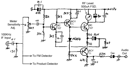
| It is perfectly possible to build a precision rectifier using an op-amp, but when this circuit was designed (1981) op amps working in the MHz range were exotic and expensive. The above circuit derives from the observation that in a complementary symmetry amplifier, each output transistor conducts only for 1/2 cycle, so the collector currents of the output emitter followers are each a precisely half-wave rectified replica of the input signal. If the amplifier has no quiescent current, but is forced into linearity by negative feedback, the precision is maintained for extremely low input levels, and audio distortion is negligible. Since the output stage has two transistors, two rectified signals are available, one being used as the audio signal, and the other as the RF level. The IF signal passes straight through the amplifier and is dumped in a 47 Ω (non inductive) resistor, the negative feedback being 100% to give overall unity gain. The signal across the load resistor should not be used unfiltered for IF output, because it contains harmonics due to crossover distortion. The two output transistors have their base voltages separated by the forward drop of a 1N4004 diode, but this is not sufficient to bias them on in the absence of signal. Note that the circuit is single-ended in respect of the audio output and therefore has little inherent supply (mains hum) rejection. For this reason, the audio is taken from the bottom of the totem pole (and the meter from the top), and the detector should be used in conjunction with a well-smoothed power supply. The circuit above, sensibly built, has a frequency response -3 dB point at about 1.6 MHz, and so is suitable for both 100 kHz and 465 kHz IFs. The audio response can be made to extend to an arbitrarily low frequency, but has a DC level proportional to carrier strength superimposed on it. Listening to the output of this detector through a set of good quality headphones is a revelation, since it demonstrates that many broadcast stations transmit signals of high fidelity within the constraints of the available bandwidth, and the distorted sound of semiconductor diode detectors is not an inherent feature of AM radio. The circuit was originally designed for use as a linear RMS sensing RF voltmeter, and further information on this application is given in a separate article. |
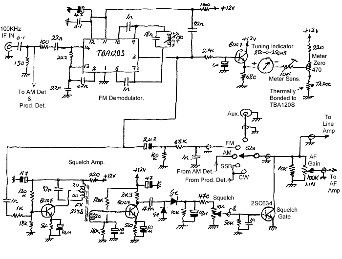
NBFM Detector, Squelch Gate, and Tuning Indicator.
|
The FM detector is a TBA120S TV sound demodulator chip adapted
to work at 100 kHz. It is now obsolete, especially with the demise
of analog TV, but still seems very popular with experimenters
(and is probably available NOS). More information on using the
TBA120 series ICs is
given in a separate article. The TBA120 / SN76660 has been around
in various incarnations since its introduction in the early 1970s;
one of the later versions being the TBA120U, which has slightly
different pinout and functionality from TBA120S shown. The author
has not tried substituting a TBA120U into the above circuit,
but there seems no reason why it should not operate perfectly
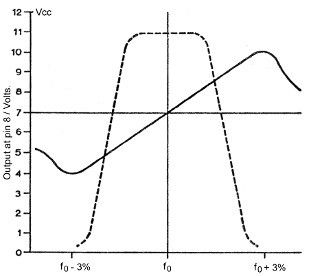
well with small changes to the circuitry as follows: 1) Pin 12 (now an audio output) should be left unconnected or used for its intended purpose. 2) Pins 4 and 5 (now remote AF gain control) should be joined together rather than ignored. 3) The bias resistor between pins 13 and 14 should be reduced to 1 kΩ or less. 4) The 22 nF capacitor between pins 8 and 11 should be re-connected from pin 8 to ground. 5) The 47 nF neutralising capacitor between pins 2 and 13 should be reduced to 22 nF. The figure below shows the DC component of the TBA120S audio output (the typical S-curve) as a function of frequency, for Q in the region of 40 - 50, with a notional IF bandpass characteristic superimposed. |
|
The output of the TBA120S discriminator is nominally centred
on 7 V; but this point varies with temperature, particularly
in the first 15 minutes after switch-on, and thermal compensation
of the tuning meter bridge is required. The thermal compensation
in the circuit above has not been fully optimised, and it is
possible that several silicon diodes in series, thermally bonded
to the IC, will give better performance in place of the original
thermistor. The TBA120U, being somewhat different in design,
may prove to have its output centred on a different voltage,
and a different (hopefully improved) thermal characteristic. The quadrature coil consists of 150 turns of 32swg enamelled wire, pile wound on a 3/16" former with a dust-iron tuning slug. The coil is housed in a 1/2" square aluminium transformer can, which reduces the Q to some extent by providing a loosely-coupled shorted turn, but even so, the circuit provides a somewhat excessive 1.9 V rms of audio for 3 kHz deviation. It may be necessary to place a resistor across the coil to reduce the output if the distortion level proves unacceptable, although distortion tends to be of low harmonic order and makes little difference to the perceived quality. Best results are obtained with the RA17 set to the 13 kHz wide selectivity position (this applies to types L, C12, C18, etc. The 8 kHz max. bandwidth of the RA17 / Mk2 is likely to give poor results). The 68k resistor between the audio output and the volume control reduces the signal to the nominally -10 dBu (220 mV rms) line level. This resistor can be adjusted according to the audio output obtained in practice, although too low a value may compromise the operation of the squelch gate. The squelch amplifier listens to the noise output of the discriminator in the region of 22 kHz, and shuts down the audio output if noise is present. The 22 kHz bandpass filter consists of a tuned transformer wound on an FX2238 (18 mm dia) ferrite pot-core, using No. 28 swg enamelled wire with turns as shown. The primary inductance is about 1.6 mH. The output of the noise amp. is rectified in a voltage doubler and used, via the squelch control, to drive the 2SC634 squelch gate transistor. Any small-signal transistor can be used for the squelch gate, although there may be some reduction in distortion to be had by connecting the collector to ground and the emitter to the audio line, rather than using the arrangement shown. Better still, the squelch gate should be replaced by an N-channel enhancement-mode MOSFET. In the original circuit, the squelch gate was connected across the volume control, affecting all of the audio outputs. This was found to serve no useful purpose, and the gate should be moved to the other side of S2a, so that it affects only the FM detector output. (An effective squelch system for AM/SSB signals must be based on the AVC (AGC) level of the receiver. The 0 to -25 V AVC output of the RA17 could be used for this purpose, but note that the AVC is intended to control the grid bias voltages of valves, it cannot stand being loaded; and so a buffer amplifier with a high input impedance will be required for sampling the AVC voltage). |
Audio Amplifier and CW Filter.
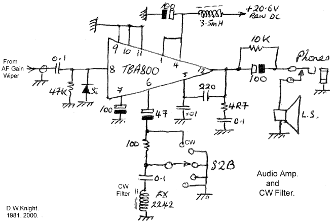
| The original audio amplifier uses a TBA800. This IC is now obsolete, and although stocks may be available, its use is not advised for new projects. Numerous alternatives are available, and circuit design is simply a matter of following the manufacturers application report for the device selected. The circuit above is included for completeness, and because the audio filter might be of interest. |
|
The audio filter arrangement was suggested to the author many
years ago by Colin Chidgey, G3YHV. It makes use of the fact that
the IC has a gain setting pin, which works by allowing the user
to shunt part of the negative feedback loop to ground with a
resistor, the gain increasing as the resistor value is reduced.
In all modes except CW, the gain setting pin is shunted to ground
with a 100 Ω resistor. In CW mode, the gain setting pin
is shunted to ground with a series resonant tuned circuit. Off
resonance, the impedance of the tuned circuit is very high and
the gain of the amplifier reduces to unity. On resonance, the
impedance of the tuned circuit is low, and the gain of the amplifier
is high. The trick, with this arrangement, is to tailor the Q
of the tuned circuit so that there is little subjective change
in volume on switching the filter into circuit (there should
be an increase in gain, but a reduction in bandwidth, so that
the subjective volume level is similar). This can be done by
making the Q as high as possible to obtain a very low dynamic
resistance, and placing resistance in series with the tuned circuit
to reduce the gain as necessary. In this example, no series resistance
was required. No details of the inductor are available because it was simply one of several surplus coils that were tried, the one used being found satisfactory. Since the resonant frequency chosen was about 800Hz, the value of the inductance can be approximated from the standard formula, ie.: f0 = 1 / 2π√(LC) This gives an inductance of about 0.4 H. The inductor is an FX2242 pot core (35 mm dia., A13 ferrite, AL = 6950 nH ±25%), completely filled with wire. Note that the core is gapped with a thin sheet of Mylar (PET) and so does not achieve its maximum AL. There is no reason why the series capacitor cannot be varied to accommodate other values of inductance. The audio filter arrangement described above can be implemented with any audio amplifier using a reasonable amount of negative feedback, provided that the amplifier is unconditionally stable for all possible values of the feedback factor (ie., lag compensation is necessary). An alternative is to use an active filter based on an op-amp, but such filters have a tendency to be noisy for a reasonable Q (12 or more), and cheap op-amps such as the 741 are grossly inadequate for the task. For those who like the idea of making audio filters using passive components, see "CW and SSB Audio Filters using 88 mH Inductors", by Ed Wetherhold, W3NQN, QEX, Dec 1988, p3-10. The high-order passive filters described by W3NQN have a relatively flat passband, and will be less susceptible to ringing than the simple LC filter used here. |
Audio Line Amplifier
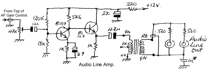
| The adapter was provided with an audio line output for recording, the two phono sockets being for connection to the standard leads supplied with stereo hi-fi equipment. The output is also perfectly suitable for connection to a computer sound card input. Complete DC isolation (strongly advised) is provided by means of a 1:1, 600 Ω line transformer. The 1 nF capacitor marked * is wired between the audio sockets and the back panel, and should be a high voltage (~1 kV) ceramic type. It was fitted to eliminate spurious radiation from the audio cables, which was audible as an increased noise level on the higher frequency ranges of the RA17. The input level preset is simply adjusted to suit the user's requirements, an output level of about -10 dBu (245 mV rms) into 10 kΩ being usual practice. |
Product Detector
|
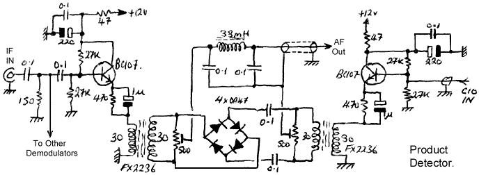
The product detector is the classic diode 'ring modulator'. Note
that the diodes are all joined anode to cathode, and the arrangement
is not the same as a rectifier bridge. The virtue of this circuit
is that it is double balanced; ie., neither the input signal
nor the heterodyning signal appears at the output, so that it
can be used to remove any audio components (noise and hum) that
might be present at the inputs. The transformers are untuned,
wound on FX2238 (18 mm dia. A5 ferrite) pot cores with turns
as shown. Screening cans are not required because the pot core
forms a closed magnetic circuit. The two 500 Ω balance
potentiometers were provided as a means for minimising the level
of input signal feed-through (in case of a mismatch of diode
characteristics, etc.), but on setup were found to optimise boringly
in the exact middle of travel. Consequently, if the circuit is
to be reproduced, it is recommended that the transformer secondaries
be wound centre-tapped bi-filar, and the pots dispensed with
altogether. Removing the 500 Ω load from each transformer
will improve the input drive sensitivity, ensuring good 'hard'
switching of the diodes. The diodes used in the original were
of type OA47, which is an archaic Ge-Au Schottky. Modern small
signal Schottkys (eg. 1N6263, IN5711) will be easier to obtain,
but practically any small diode will work at 100 kHz. The truly
obsessive will seek to match the characteristics of the 4 diodes,
but choosing all from the same batch is probably sufficient.
A simple measure of balance with respect to the IF input can
be had by removing the CIO feed and seeing how much audio emerges.
AM rejection should be easily better than 35 dB. The two inputs
are interchangeable, so CIO input balance can also be checked
by applying the IF signal to the CIO input. Note that the balanced modulator has two apparently redundant 0.1 μF capacitors in series with the outputs of one of the transformers. These capacitors force the diode working points into balance and improve carrier and AM rejection performance considerably (see "Improving the doubly-balanced mixer", Tech Topics, Rad Com, Dec 1980, p1292). |
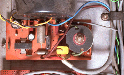
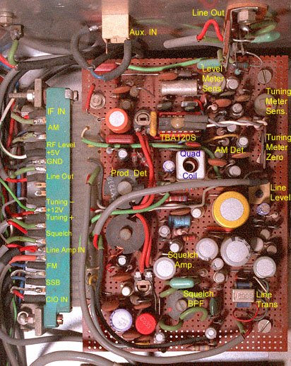
Layout of the Prototype Demodulator and Line Amp. Board.
Audio construction methods are perfectly adequate for circuitry operating at 100 kHz.
» Part 3.
D.W. Knight. 1981, 2000, 2002, 2014
Home | Ra17 index || prev | next |
u