|
|
|
|
|
|
|
1. Prototype magnitude bridge. 2. Insertion defect. 3. Load-side voltage sampling. 4. Port balancing. 5. Capacitor-compensated RVS. 6. Capacitive voltage sampling (CVS). |
7. . 8. Detectors and comparators. 9. Summing networks. 9a. Logarithmic meter response. 10. Absolute measurements. 11. . |
|
Introduction: As has been stressed in [Impedance Matching], the traditional SWR-meter is an inadequate diagnostic for the adjustment of antenna-matching networks because it gives no information regarding which network component should be adjusted or the direction in which the adjustment should be made. Far better information can be obtained by using a class of circuits that we will refer-to here as Magnitude-Difference Bridges (MDBs); i.e., bridges that use a pair of detectors to compare the magnitudes of linear-combinations (i.e., sums and differences of multiples) of voltage and current samples taken from a transmission-line. As will be shown in the discussion to follow; it is possible, by suitable choice of linear-combinations, to devise passive analog computation methods for any attribute of a load impedance in isolation from its other attributes. Thus we can devise bridges that register magnitude ( |Z| ), phase (φ), resistance (R), conductance (G), or any other impedance-related quantity, and give an indication of the direction in which the quantity needs to be adjusted in order to meet a target value. Such bridges can be used as adjustment-specific indicators for the purpose of manual impedance-matching; or just as easily, can produce voltages for feeding to servo-amplifiers or level-detectors as part of an automatic antenna-matching system. A combination bridge giving null indications of R, G and φ in relation to a target load impedance was dubbed a "Match Meter" by Nigel Williams. The Match Meter, based on principles outlined by Underhill and Lewis [43], was introduced conceptually in [Impedance Matching] as a means by which an initially encountered load impedance can be assigned to a region of the Z-plane, thereby identifying firstly: the most appropriate matching network configuration (if selectable): and secondly, the adjustments necessary to effect a transformation to the target load impedance. One particular virtue of the Match Meter is that it resolves the inherent ambiguities in the adjustment of T and π networks (which have three controls for solving a two-dimensional problem), but it will guide the adjustment of any network capable of producing a match. The outcome is a procedure that is always convergent (i.e., it will never fail provided that the matching network has sufficient adjustment range); and that is maximally efficient insofar as the shortest route through the Z-plane constitutes the best matching solution using a given network (which it usually does). In this section we will establish the design considerations for magnitude-difference bridges in general, and R, G and φ bridges in particular. We will also include, and indeed start with the impedance magnitude ( |Z| ) bridge: firstly because the |Z| bridge is the most basic MDB and informs the design of the others; and secondly because |Z| is the criterion governing the choice of impedance transformation ratio (when adjustable) and therefore provides important information. The principle of the magnitude bridge as deduced from the Wheatstone-Christie prototype was introduced in [Bridge principles]. Here however, we will concern ourselves mainly with current-transformer bridges, since the objective is to make minimally-invasive devices for insertion into transmission lines. |
|
1. Prototype Magnitude Bridge: Shown below is a generic scheme for a current-transformer magnitude bridge. A generator delivers power to a load impedance Z, and the process is intercepted by a current-sampling network, which produces a voltage Vi, and a voltage sampling network, which produces a voltage Vv. The networks are calculated so that when the load impedance magnitude |Z| is equal to the target load resistance R0, the magnitudes of the two sample voltages are equal. The two samples are rectified and subtracted. Neglecting loading effects and losses (to be discussed later), and assuming the use of simple diode detectors; rectification of a voltage Vx (x being either i or v in this case) produces a DC voltage of ±[ (√2)|Vx| - Vf ] , where Vf is the forward voltage drop of the diode. Assuming that the two detectors are effectively identical (apart from diode polarity) and that there is enough RF drive to turn the diodes on; the diode losses are cancelled by the subtraction process and the output is a DC voltage proportional to |Vv|-|Vi| . If we (say) arrange things so that Vv drives the DC output positive and Vi drives the output negative; the output will be positive when |Z|>R0 and vice versa. |
| The sampling-network design requirements for frequency-independence of the balance condition can be satisfied by choosing the networks as if designing an ordinary impedance bridge. The potential divider used to obtain Vv can be a pair of resistors with an inductor across the lower arm to compensate for the secondary inductance of the current transformer; or it can be a pair of capacitors with a compensation resistor across the lower arm. It is also possible to implement maximally-flat voltage and current sampling networks [see: Maxflat transmission bridges] in the event that constant sensitivity is required. We should note however that, for a magnitude bridge, the frequency responses of the two networks only need to be identical in terms of magnitude (whereas for an impedance bridge the responses must be identical in both magnitude and phase). This permits a certain relaxation of the design rules. For example, it is possible to make a voltage sampling network that tracks the magnitude response of the current transformer by using a resistive potential divider with a capacitor in series with the upper arm (as opposed to an expensive and troublesome inductor in parallel with the lower arm). Also, we do not need to worry too much about the high-frequency phase-error of the current transformer (provided that is not so large as to affect the output magnitude); for which reason the transformer secondary parallel capacitance has not been included in the model shown above. We must not assume however, that any balance imperfections will be swallowed by the diode threshold effect. As implied before, it is best practice to arrange things so that the diode characteristic is cancelled by the summing process, in which case the DC output is linear. More to the point, an MDB measures the difference between two relatively large voltages, and so, unlike an SWR bridge, which works by rectifying the Vv-Vi output of an impedance bridge, it can measure arbitrarily small balance errors. |
|
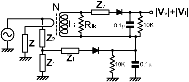
2 Insertion Defect: The necessary balance condition for a perfect magnitude bridge is: |Vv| = |Vi| when |Z| = R0 It is natural to assume that we can satisfy this requirement by arranging things so that: Vv = Vi when Z = R0 in which case, the basic AC design considerations are exactly the same as for an ordinary impedance bridge and we can select our design equations from analyses carried-out elsewhere. There is a subtle error in this assumption however, which stems from the fact that when |Z|=R0, it is not necessarily true that Z=R0. It is perfectly possible to have |Z|=R0 when Z is highly reactive. Thus, we will be advised to perform an analysis specifically for the magnitude bridge, to see where the analogy breaks down. The problem, as it will transpire, is associated with the current-transformer, and so we can leave the voltage-sampling network in generic (Z1, Z2) form while uncovering it. For a toroidal current transformer with a ferrite or iron-dust core, the coupling coefficient is close to unity. Hence (with reference to the diagram above), noting that I=V/Z, we can obtain an expression for Vi by applying the ampere-turns rule: Vi = I Zi / N = V Zi / (N Z) . . (2.1) where N is the turns ratio and Zi is the total secondary load impedance defined as: Zi = Rik // jXLi Li is the effective or 'coupled' secondary inductance (i.e., the measured inductance minus the leakage inductance). Rik is the effective secondary load resistance (allowing for core losses, i.e., Rik=Ri//Rk, where Ri is the actual load resistance, and Rk is the loss resistance). The output of the voltage sampling network is: Vv = V' Z1 / (Z1 + Z2) . . (2.2) But this voltage is derived from the generator voltage V', whereas we require an expression derived from the load voltage V; the point being that voltage can be eliminated from the balance condition if the current and voltage samples are related to the same reference. Hence we note that V' differs slightly from V due to the insertion impedance of the current transformer Zii. Thus: V' = V + Vii = V + I Zii = V + V Zii / Z Zii is, of course, to a very good approximation, the secondary load impedance scaled down by the square of the turns ratio. Hence: V' = V [ 1 + Zi / (N² Z) ] Substituting this into (2.2) gives: Vv = V [ 1 + Zi / (N² Z) ] Z1 / (Z1 + Z2) . . . . (2.3) When the bridge is balanced, |Vv|=|Vi| and |Z| → R0. To derive the balance relationships, we start by equating the magnitudes of (2.1) and (2.3) and cancelling V: | Zi / (N Z) | = | [1 + Zi / (N² Z) ] Z1 / (Z1 + Z2) | This is the familiar balance condition for an ordinary impedance bridge, except that it is in magnitude form. To deal with this situation using the minimum number of logical steps, we can use an algebra specific to magnitudes, as was set out in [AC Theory, 24]. A magnitude expressed as the ratio or product of phasors remains true when all of the phasors are replaced by their magnitudes [AC Theory, 24.1 and 24.3]. Hence we can convert all of the impedance or admittance factors directly into magnitudes and still satisfy the balance condition (this is the reason why we have additional frequency-response compensation options in comparison to the ordinary impedance bridge). Hence: |Zi| / (N |Z|) = | 1 + Zi / (N² Z) | |Z1| / |Z1 + Z2| The instance of |Z| that has appeared on the left can now be replaced by R0. Also we can get the equation into a more tractable form by taking reciprocals of both sides and rearranging. Note, as we do so, that the reciprocal of a magnitude of a phasor is equal to the magnitude of its reciprocal [AC Theory, 24.2]. |
|
|Z1| |
|
|
|
N² Z |
|
|Zi| |
| Now we can multiply-out the right hand side, and we have two options in the matter of how to do that. We can either leave 1/|Zi| as a magnitude as we multiply it into the magnitude bracket to its left [AC Theory, 24.4], or we can convert it back into an admittance [AC Theory, 24.3]. We will choose the latter option because it will allow us to cancel Zi from the rightmost term. |
|
|Z1| |
|
|
Zi |
|
N Z |
|
|
Now we can see the problem. For the impedance bridge, we can
always replace Z with R0 at the
balance point; but for the magnitude bridge, we can only replace
|Z| with R0. The instance of Z
on the right hand side cannot be factored out as an individual
magnitude because it makes separate contributions to the real
and imaginary parts of the sum within the magnitude bracket.
This means that, for the current-transformer magnitude bridge,
there is no universal solution for the balance condition. We
can only get solutions of the form: |Z| = R0 ± δR where δR is a frequency-dependent error-term that varies according to the reactive content of Z. This is more a design issue to be aware of however, than an actual cause for concern. The point to notice is that the term in which Z appears is merely a small correction for the current transformer insertion impedance (Zii=Zi/N²). This means that the error term can be made arbitrarily small by minimising the insertion impedance (i.e., by using a low value of Rik or a large N). Zii must be finite however if the bridge is to have useful sensitivity. We might therefore choose to eliminate the correction term by moving the voltage sampling point to the load side of the transformer, but this will probably make matters worse as we shall see later. Some may even be tempted to strike-out the correction term altogether, on the grounds that the model error will usually be less than 1%; but in fact the optimum solution is to make the substitution that gives the minimum systematic error. This corresponds to the balance condition: |Vv| = |Vi| when |Z| = R0 ± δR AND δR → 0 when Z → R0 which is, of course, the same as adopting the balance criterion: |Vv| = |Vi| when Z = R0 Hence we can substitute R0 for Z in the equation above to obtain the best compromise: |
|
|Z1| |
|
|
Zi |
|
N |
|
|
This is equivalent to adopting the magnitude form of the solution
for the full impedance bridge; and therefore confirms that we
are at liberty to use existing impedance-bridge design equations
in order to choose networks and component values. For those who are concerned about the inherent imperfection in the current-transformer magnitude bridge, it should be noted that the defect will make no practical difference in the context of antenna matching, even when a bridge of high sensitivity (significant Zii) is required. The reason is that the set of diagnostic bridges used always includes a phase bridge. The phase bridge ensures that Z is (very nearly) purely resistive as the matching solution is approached, while a magnitude bridge (say) ensures that |Z| → R0. Hence, overall, Z → R0, and the error disappears. All current-transformer MDBs have the defect, but the action of the bridges in concert permits replacement of Z with R0 whenever it cannot be eliminated from the insertion-impedance correction term. Note that the Wheatstone-derived magnitude measuring bridge [Bridge principles] does not have the insertion defect, and so is the better choice when making two-terminal measurements of impedance magnitude. The final generic form for the balance condition of the magnitude bridge is obtained by putting the equation above into a form from which the magnitude of the right-hand side can be calculated. This can be done by noting that 1/Zi=(1/Rik)+(1/jXLi). Hence: |
|
|Z1| |
|
|
Rik |
|
jXLi |
|
N |
|
|
| The magnitude is evaluated using Pythagoras' theorem: |
|
|Z1| |
|
|
|
Rik |
|
N |
|
2 |
|
|
XLi |
|
2 |
|
| Analytical progress from this point depends on the choice of voltage sampling network. Note however that, once the choice is made, the left-hand side can also be put into a form that is the square-root of a sum of squares. Hence both sides can be squared to get rid of the square-root symbols. The trick is to choose networks so that the sums separate cleanly into frequency-dependent and frequency-independent parts. Then the balance condition can be separated into two (or more) equations that can be solved for the component values, provided that frequency-independent solutions exist. |
|
3. Load-side voltage sampling: One way to eliminate the insertion impedance from the balance condition is to take the voltage sample from the load side of the transformer. In that case, the voltage sample takes its reference from the load voltage V, i.e.; |
|
Vv = V Z1
/ (Z1 + Z2) The downside however is that the current flowing in the transformer primary is now: I' = V / [ Z // (Z1 + Z2) ] This causes the expression for the current sample to come out as: |
 |
|
Vi = I' Zi
/ N = V Zi / { N [ Z
// (Z1 + Z2)
] } Equating the reciprocals of the magnitudes of the voltage and current samples and cancelling V gives: |
|
|Z1| |
|
|
Zi |
|
| This is the condition which we wish to apply exactly when |Z| = R0, but once again we cannot factor |Z| cleanly from the right-hand side. Hence there is no exact solution for the load-side voltage sampling case either, and instead of an insertion defect we have a shunt defect. The issue however, is whether we can achieve a solution that gives the minimum systematic error. To find out, we can expand the parallel product in the expression above and apply the magnitude product rule [AC Theory, 24.3]: |
|
|Z1| |
|
|Zi| |Z + Z1 + Z2| |
| This gives a useful cancellation and extracts an instance of |Z| that can be replaced with R0. After rearrangement we get: |
|
|Z1| |
|
|Zi| |
| Now we can see that the rogue instance of Z operates additively on the series combination Z1+Z2. To get the bridge to balance correctly when Z=R0, we must therefore include R0 as an offset when determining Z1+Z2. The consequence is that, unless we add more complexity to the circuit, we can only obtain a frequency-independent solution for the balance condition if Z2 has a series resistive component, or if Z1 is purely resistive. To illustrate this point, we can start by expanding the right-hand side: |
|
|Z1| |
|
|
|
Rik |
|
jXLi |
|
| The choice of networks must be such that the left-hand side can be put into a form that has the same frequency dependence as the right-hand side; i.e., it must be possible to arrange it as a series of terms within a magnitude bracket, with any number of frequency-independent terms, and a single term having either a pure capacitive reactance in the numerator, or a pure inductive reactance in the denominator (to compensate for XLi). Using the magnitude ratio rule [AC Theory, 24.1], we get the appropriate form: |
|
|
Z1 |
|
Z1 |
|
|
|
|
Rik |
|
jXLi |
|
|
| Now, the objective is to get a single term on the left hand side that has the factor 1/(2πf) in it. If we make Z1 a resistor, i.e., Z1=R1, then we can get the required frequency compensation by making Z2 a resistor in series with a capacitor, i.e. Z2=R2+jXC2. The balance condition becomes: |
|
|
R1 |
|
R1 |
|
R1 |
|
|
|
|
Rik |
|
jXLi |
|
|
And the solution, after taking the sums of the squares of the
reals and imaginaries on each side and equating frequency-dependent
and frequency independent terms (and recalling that XC=-1/(2πfC) and XL=2πfL), is: |
|
1 / (C2 R1) = N
R0 / Li and (R0 + R1 + R2) / R1 = N R0 / Rik |
| We can also use the familiar inductor-compensated resistive voltage-sampling scheme, which works for ordinary impedance bridges. In this case Z1 becomes a resistor in parallel with an inductor, i.e., Z1=R1//jXL1, and Z2 is a resistor R2. This gives the balance condition as: |
|
|
1 + (R0 + R2) |
|
R1 |
|
jXL1 |
|
|
|
|
|
Rik |
|
jXLi |
|
| And the solution is: |
|
(R0 + R2)
/ L1 = N R0 / Li and (R0 + R1 + R2) / R1 = N R0 / Rik |
| What we cannot do however is obtain a convenient frequency-independent solution in the case where the voltage-sampling network is a capacitive potential divider with a compensating resistor across the lower arm. In that case Z1=R1//jXC1, and Z2=jXC2. The balance condition is then (expanding 3.1 and noting that XC2/XC1=C1/C2): |
|
|
R1 |
|
jXC1 |
|
R1 |
|
C2 |
|
|
|
|
Rik |
|
jXLi |
|
|
We are left with the term R0/jXC1, which has no counterpart on the right-hand
side. We may, of course, choose to neglect it on the grounds
that |XC1|>>R0;
but in fact, that is a rather poor assumption. We cannot make
|XC1| arbitrarily large at the highest
frequency of operation because, unlike the ordinary impedance
bridge, the voltage and current sampling outputs remain on load
(driving individual detectors) when the bridge is balanced. Hence
we must achieve a usefully low output impedance for the voltage-sampling
network; which means, in practice, that for a 4 to 5 octave bandwidth,
|XC1| will be only a few hundred Ohms
at the highest frequency and the error will be of the order of
10% (assuming R0=50Ω). There is a solution however, albeit not a very prepossessing one, which involves including a capacitor in parallel with either the primary or the secondary of the current transformer. Assuming that we place the capacitor (Ci) across the secondary (a capacitor across the primary would have to be N² times larger), the secondary parallel impedance becomes: Zi = Rik // jXLi // jXCi This gives a new balance condition: |
|
|
R1 |
|
jXC1 |
|
R1 |
|
C2 |
|
|
|
|
Rik |
|
jXLi |
|
jXCi |
|
| Now we have a frequency-response counterpart for R0/jXC1, and the solution is: |
|
C1 = N Ci 1 / (C2 R1) = N R0 / Li (R0 / R1 ) + 1 + C1 / C2 = N R0 / Rik |
|
But there is a practical problem. There will already be an effective
capacitance Ci in parallel with the transformer
secondary due to propagation-delay and through-line mismatch.
This capacitance can be either positive or negative, but is typically
of the order of 10 pF if a Faraday-shield is used. In order to
keep the generator power-factor reasonably close to unity, we
will want to make C1 less than about 14
pF (for input SWR < 1.2 at 30 MHz). If the transformer has
(say) 14 turns, then we will need to get Ci
down to about 1 pF. The only way in which to do that is to neutralise
the transformer, a practice that adds considerable complexity
to the circuit. It must also be said that, since we see no phase
information in the bridge output, the neutralisation process
will interfere with the business of balancing the inductance
in the arms of the voltage-sampling network (to be discussed
later); i.e., we will end-up with too many adjustable frequency-response
parameters. In mitigation however, it will be possible to compromise
the inductance-balance adjustment, to give an approximate response
correction in the absence of neutralisation, which will be good
enough for most purposes. It is not possible to say that load-side voltage sampling is a bad idea, but in general, it is somewhat more troublesome than generator-side sampling and offers no cure for the insertion defect. It could be argued of course, for the case where the bridge is left permanently connected at the input to an antenna matching network; that the sampling network can simply be regarded as part of the antenna-system input impedance and the shunt defect is effectively eliminated. Unfortunately however, the bridge must be calibrated somehow, and that will involve connecting it to a reference load-resistor; in which case the shunt defect will be present and will skew the calibration. |
|
4. Port balancing: Although the theory required for the design of magnitude bridges (and other MDBs) is closely related to that of ordinary impedance bridges; there is a specific (and generally neglected) design issue that can have a serious effect on accuracy. This is that the voltage and current sampling outputs (the ports) remain on load when the bridge is balanced; which means that the detector input impedances play a part in determining the balance condition. Worse still, diode detectors are non-linear, which means that their input impedances vary with drive level (see [Diode detectors, section ?] ). Hence, for the prototype bridges considered so far, the balance point will drift as the generator (transmitter) output is varied. The basic workaround for the port loading problem is to try to make the detector input impedances as high as possible. We might, for example, use detector load resistors of several hundred kΩ and feed the outputs into high-impedance DC amplifiers. Alternatively, we might connect high-impedance RF buffer amplifiers between the ports and the detectors. These methods however, are complicated and require DC power supplies (i.e., they fail to make use of the rather large amount of energy that is usually available). Another workaround is to include an auxiliary RF level-detector and insist that the balance point should only be determined when when the level is between certain limits. This however, is another complicated solution, and is unergonomic if the level has to be set manually. We should also take exception to the fact that, if the bridge is to be left in line during radio transmissions, the null reading will vary in the presence of SSB and other discontinuous signals. A well-designed automatic matching system should be able to find a solution using any signal of reasonably narrow bandwidth, and we certainly don't want it re-triggered falsely once a solution has been found. There is however, a general solution to the detector loading problem that we will refer to here as port balancing. It involves placing an impedance equal to the output impedance of the voltage-sampling network in series with the current-sample output, and vice versa. In this way, both networks will have exactly the same output impedance, and will be equally susceptible to loading effects. The beauty of this method is that, if both detectors have the same input impedance (which they will have to a very good approximation if well-matched diodes are used), then they cannot affect the balance condition, no matter how low the input impedance is (they can, of course, still affect the off-balance response, but that is a much less serious issue, and is usually irrelevant in antenna-matching applications). Hence, if we include port-balancing networks, we do not need to re-calculate the sampling networks to allow for detector loading. Further good news is that the networks are passive, and the required component values can be deduced by inspection. |
|
The output impedance of a potential
divider was derived in [AC Theory, 36]. Neglecting the
generator output impedance (which makes no contribution to the
bridge balance condition and can therefore be ignored in this
context) it is given by the parallel combination of the impedances
in the upper and lower arms. Hence, the port-balancing impedance
in series with the current-sample output is simply: Zv = Z1 // Z2 |
 |
|
If Z2 is provided by (say) a capacitor
C2, and Z1
is provided by a resistor Rv in parallel
with a capacitor C1, then Zv is provided by a resistor Rv
in parallel with a capacitor of value equal to C1+C2. The output impedance of a current transformer was derived in [Current transformers, section ?]. This, to a very good approximation is identical to the secondary load impedance, i.e., the transformer reactance in parallel with the load resistance. Hence the port compensating impedance for the voltage sample can be a toroidal inductor identical to the transformer secondary in parallel with the same value of resistor as that loading the transformer (i.e., the same as the actual resistor Ri, not the effective resistance Rik - the core will provide the loss component). One additional issue in the matter of port-balancing is that the sensitivity of a diode detector is partially determined by the DC resistance looking back into the port to which it is connected. Essentially, the DC resistance is a component in determining the currents that flow in the detector load and any measuring circuits attached, to the extent that the sensitivity goes to zero when the DC path is open-circuit. Hence we must also ensure that both ports have the same DC resistance to ground. The DC port-balancing requirement is taken care of automatically when a capacitive potential divider with an LF compensating resistor is used. There can be a problem however when the upper voltage-sampling arm Z2 has DC continuity. The issue is that some radio transmitters have a DC blocking capacitor in series with the output, and antenna tuners and antenna systems quite often have no DC path across the input terminals. The solution is to place a DC blocking capacitor in series with Z2 (a 10 nF or 100 nF high-voltage ceramic capacitor will usually do the trick), and to include a corresponding capacitor in the port-compensation network for Vi. (The alternative of placing an RF choke across the generator is too horrible to contemplate). This issue is associated with bridges that use a resistive potential divider and have no LF compensation coil across the lower arm, i.e., bridges designed for only moderate precision or for a restricted frequency range. If a compensation coil is used, the DC resistance looking back into the port will be practically zero and the resistance looking back through Z2 into the generator will have no discernible effect. Note that for AC port-balancing, it is only strictly necessary that the two outputs should have the same magnitude of output impedance. Calculating alternative networks on that basis however is likely to complicate the DC balancing, and is probably not worthwhile. |
|
Single-impedance port-balancing: In some cases, there may be a port-balancing solution that requires only a single impedance to be placed in series with the port having the lowest output impedance (usually the current-transformer). This occurs when it is possible to compute a physical network that has the impedance: Zcomp = Zv - Zi the point being that, in terms of equalising the output impedances, placing a positive impedance in series with one port is the same as placing a negative impedance in series with the other. |
|
A single impedance solution is
possible when a resistive voltage-sampling (RVS) network with
a compensating inductor is used. This is perhaps not the most
prepossessing of design options in most circumstances, but it
serves to illustrate the idea. The balance condition for this
bridge is obtained by substituting the voltage-sampling network
parameters into equation (2.4),
i.e., using: Z1 = R1 // jXL1 |
 |
|
and Z2=R2, we get: |
|
|
R1 |
|
jXL1 |
|
|
|
Rik |
|
N |
|
jXLi |
|
|||
|
From this we can see by inspection that: R2 / L1 = N R0 / Li i.e.; L1 = R2 Li / ( N R0 ) . . . (4.1) and (R1 + R2) / R1 = ( N R0 / Rik ) + 1/N Here we can observe that port-compensation is not as critical as establishing the balance condition; and so for the purpose of establishing the resistive component of the voltage-sampling network output impedance, we can make the approximation that the current-transformer has zero insertion impedance. This allows us to delete the 1/N term in the equation above. (For a transformer with N>10 and R0=Rik, the error is <1%). Thus, to a good approximation: (R1 + R2) / R1 = N R0 / Rik Now notice that if we divide both sides by R2, the left hand side becomes the reciprocal of R1//R2 : (R1 + R2) / (R1 R2) = N R0 / (Rik R2) Hence: R1 // R2 = Rik R2 / ( N R0 ) Comparing this with (4.1) above, we see that there is a common factor: (R1 // R2) = Rik [R2 / (N R0)] and L1 = Li [R2 / (N R0)] Hence: Zv = R1 // R2 // jXL1 = [R2 / (N R0)] ( Rik // jXLi ) = [R2 / (N R0)] Zi Zv is simply a scaled-up version of Zi, and so our port-compensating impedance Zv-Zi is: Zcomp = [R2 / (N R0)] Zi - Zi i.e.: Zcomp = Zi ( [R2 / N R0] - 1 ) Zcomp being made up from an inductor in parallel with a resistor, their values being: Rcomp = Rik ( [R2 / N R0] - 1 ) and Lcomp = Li ( [R2 / N R0] - 1 ) |
|
Production engineering: It is better to design accurate bridges and ruin (sorry, rationalise) them for production purposes, than it it to design inaccurate bridges and try to get them to work during the production process. As alluded to earlier, port compensation does not have to be carried out as accurately as does setting-up the balance condition. When the detector input impedances are 'reasonably high', it is a fairly minor correction. Hence, although it is important to be aware of the port-balancing issue, it is not always necessary to include all of the components. The approach recommended is to start with a candidate circuit that gives the minimum systematic error, and then delete any components that have negligible effect. The most important port-compensation requirement is that of the DC resistance, which sets the gains of the detectors. The AC requirement, on the other hand, may obviously be relaxed if both ports have relatively low output impedances. Also, as is usually more relevant in practice: if there is a considerable difference between the output impedances of the two ports; it is more important to pad the low-impedance port than it is to place a small impedance (which will make hardly any difference) in series with the high-impedance port. A case in point is the capacitive potential divider, which can have an output-impedance magnitude of many hundreds of ohms at low frequencies. Placing a network equivalent to the output impedance of a current transformer in series with that will often have little beneficial effect. Hence we can save costs by omitting an inductor in parallel with a resistor, while still including the important padding network in series with the other port. Another point concerning the reduced accuracy requirement of port compensation in comparison to that of establishing the balance condition, is that the voltage-sampling network will usually (or should) be adjustable so that the bridge can be calibrated. Hence, strictly, the output impedance will not be established until calibration has been carried out. If the circuit model is reasonably accurate however, the calibration values will not differ greatly from the calculated values, and so the latter will suffice for determining the corresponding port-balancing network. |
|
5. Capacitor-compensated resistive voltage-sampling. As mentioned earlier, when tailoring the frequency-responses of the voltage and current sampling networks, it is only necessary to establish identical magnitude responses. In discussing the generic balance condition earlier, it was noted that this requirement can be met by placing a capacitor in series with the upper arm of a resistive voltage-sampling (RVS) network. In that case: Z2 = R2 + jXC2 and Z1 = R1 and the balance condition (2.4) for a bridge with generator-side voltage sampling becomes: |
|
R1 |
|
|
Rik |
|
jXLi |
|
N |
|
| It can be seen by inspection that the network solutions are: |
|
1 / (R1 C2) = N R0 / Li i.e.:
and
The corresponding circuit is shown on the right; with optional port-balancing networks, and an additional capacitor C1 for high-frequency compensation (to be discussed shortly). |
 |
|
To get a feel for the component values, take for example a fairly
typical bridge using a 1:12 current transformer (i.e., N=12)
having a secondary inductance of 9 μH, with Rik=50
Ω and R0=50 Ω. In this case,
the ratio R2/R1
needs to be 11.083. If we choose R2=3.9
kΩ, then R1=3900/11.083=352 Ω
and C2=Li/(NR0R1)=42.6 pF. C2 turns out to be a small capacitance because
R2 is a relatively large resistance. The trimmer C1 is included to balance the parasitic reactances of the arms of the voltage-sampling network at high frequencies. The high-frequency response of a resistive potential divider is usually dominated by the parallel capacitances, and for the response to be flat, the two reactances need to be in the same ratio as R2/R1. The parallel capacitance of R2 will be about 0.5 pF, and so the total C1, including strays, needs to be adjusted to about 0.5×11.08 = 5.5 pF. In practice however, C1 will be adjusted to give a response that falls very slightly at high-frequencies. The reason is that there will be some parallel capacitance across the current-transformer secondary, which will cause its response to fall. Hence, by slight over-adjustment, C1 can match the HF amplitude response of the voltage sampling network to that of the current-sampling network. Notice overall, that the bridge has three balance adjustments, which have to be set when a 50 Ω or other preferred reference resistor (R0) is connected in place of the load. C2 sets the balance at the low-frequency end of the working range, R1 in the middle, and C1 at the high-end. Three-point frequency tracking can easily give a calibration precision better than ±0.1% over the 1.6 MHz to 30 MHz range (accuracy depends on the uncertainty in the known value of R0). |
|
6. Capacitive voltage-sampling. For cool running and the abstraction of the minimum amount of power from the through-line, the capacitive voltage-sampling network (CVS) is usually the best choice. In this case, Z2 is provided by a capacitor C2, and Z1 by a capacitor in parallel with a resistor; i.e.; Z2 = jXC2 and Z1 = R1 // jXC1 When the voltage-sampling network is on the generator side, the balance condition (2.4) becomes: |
|
|
|
C2 |
|
R1 |
|
|
|
Rik |
|
jXLi |
|
N |
|
The solutions are:
and
|
| A practically realisable circuit is shown on the right, with port-balancing networks (if required), and additional compensating inductors L2 and Lα. Adjustment of C1 establishes the basic potential-divider ratio and so is used to set the balance-point in the middle of the frequency range. R1 compensates for the finite inductance of the current-transformer secondary and so sets the balance-point at low frequencies. The coil Lα in series with the generator is for input power-factor (PF) correction, i.e., it compensates for the capacitance that the voltage-sampling network places across the through-line. The coil L2 is used to balance-out the parasitic inductance of Z1, thereby adjusting the bridge balance-point at high frequencies. |
 |
|
The best way to construct the bridge
is to make the through-line from coaxial cable, with one or more
gaps in the outer shield and dielectric to allow the current-transformer
to work and to permit connection of the voltage-sampling network.
The stub of cable passing through the transformer-core acts as
a Faraday shield (and is called 'the Faraday shield'), but it
also helps to maintain the average characteristic-resistance
of the through-line (which should be the same as R0).
For a lossless line: R0 = √(L0/C0) Where L0 is the inductance per unit length and C0 is the capacitance per unit length. The effect of making gaps in the shield (assuming chassis continuity between the generator and load ports) is to give a slight excess of inductance and thereby raise the average characteristic resistance. The effect of connecting a capacitive network across the line, on the other hand, is to give a significant excess of capacitance, and thereby reduce the average characteristic resistance. Fortunately, we can largely correct for such imbalances by using lumped components, provided that the resonant-frequency of the lumped series inductance and the lumped parallel capacitance is several times greater than the maximum operating frequency. At high frequencies, when the resistance R1 is large in comparison to the magnitude of XC1, and ignoring L2 (which will have a small reactance in comparison to |XC2| ), the capacitance looking into the voltage-sampling network from the generator will be: Cvs = C1 C2 / (C1 + C2). Hence, when the impedance matching process is complete and the line is terminated in R0, we can obtain unit power-factor for the generator by arranging things so that: √[(Lα - Lgap)/Cvs] = R0 where Lgap is the small excess inductance due to the various gaps in the outer shield. Generally, when designing a CVS bridge which has no input PF-correction, it is good practice to keep the generator phase-angle within ±7° (SWR <1.2) when the load is matched. For a 50 Ω system, this means that |XCvs| should be <407 Ω, which means that Cv should be 13 pF or less for operation up to 30 MHz. This is still a sensible rule to apply even when PF-correction (Lα) is included, because it ensures that resonance of the lumped transmission-line elements will occur at >>30 MHz. To give an idea of practical component values, we will use the same current transformer example as in the previous section, i.e.: N=12, Li=9 μH, Rik=50 Ω and R0=50 Ω. If we choose C2=12 pF, then (6.1) gives C1=133 pF and (6.2) gives R1=1250 Ω. Cvs=11 pF and so Lα=R0²Cvs=27.5 nH assuming that the gap inductances are negligible. The series-resonance disaster occurs when: f =1/[2π√(LαCvs)=290 MHz and so will never cause a problem except under conditions of extreme misuse. Lα is a tiny coil made by winding about 2 turns of the coaxial-cable inner-conductor around the shank of a drill-bit or a small screwdriver. Its dimensions can be computed using Wheeler's formula. The inductor L2 corrects for the parasitic inductance of the lower voltage-sampling arm. It has practically no effect at low frequencies, and so can be adjusted with minimal interaction to set the balance-point at high frequencies. For the voltage-sampling network to have a flat frequency response (neglecting the LF compensation resistance R1) it is necessary that the inductive reactances in the arms of the network are in the same ratio as the capacitive reactances, i.e; L2 / L1 = C1 / C2 where L1 is the parasitic inductance of the lower arm. With good construction (very short wires) it is possible to get L1 down to something in the region of 20 to 25 nH. If L1 is (say) 25 nH, then L2 total (including the parasitic inductance of the upper arm) will be 277 nH for our example bridge. A small coil (5 or 7mm diameter former) with 3 or 4 turns and a dust-iron slug will do the trick. Note that the adjustment of L2 will automatically correct for any minor HF-response error of the current transformer during the calibration process. The output impedance of the voltage-sampling network (Zv) can be represented as a capacitance C1+C2 in parallel with a resistance R1. For the example bridge, this is 145 pF//1.25kΩ. At 1.6 MHz this gives: Zv = 1250 // -j686 Ω If we use a diode detector with a load resistance of (say) 10 kΩ, then the detector input resistance will be a few % greater than (10K+1250)/2 = 5.63 kΩ. Such a load will definitely make the voltage-sampling output droop, and so the port-balancing network in series with the current-sample output will be required. At 30 MHz, the output impedance of the VS network will be: Zv = 1250 // -j36.6 Ω Detector loading will not be a serious problem at this frequency. The magnitude of the output impedance of the current-sampling network will always be 50 Ω or less. Hence failure to compensate for it will give rise to an error of 1% or less when driving a detector of 5 kΩ input resistance. Thus the port-balancing network in series with the VS output will make a small improvement to the balance accuracy, but it is unlikely to survive a visit to a production-engineering department. |
|
7. Transformer voltage-sampling: >>> Not written yet. Further experimental work to be undertaken. >>>>>>>> . |
|
8. Detectors and comparators: There are numerous possibilities for rectifying and using the outputs of a magnitude-difference bridge, and it is not possible to report them all. The examples given below however illustrate most of the important design considerations. |
|
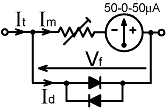
The circuit on the right is a fairly typical arrangement for
driving a centre-zero meter. The detector load resistances are
chosen to be relatively low, the reason being that the detectors
must be able to source and sink current. The direction of the
current flowing in the meter is dictated by whichever detector
is producing the highest output voltage, and the load resistor
of the other detector provides the DC path to ground. As shown,
the meter needle will move to the right when: |Vv| > |Vi| |
 |
| In order to produce a control-voltage for use in an automatic impedance-matching system, the diodes are connected so that the detectors produce voltages of opposite polarity, and the voltages are summed using a resistor network. Shown below are two such summing circuits; one being popular but problematic, the other being the best choice in most circumstances. |
|
If it is not immediately obvious, the circuit on the left provides
a bridge-balance adjustment that will interfere-with the process
of calibration. It is best to establish the balance-condition
by adjusting the RF sampling parameters; in which case the trim-pot.
is redundant and invites mis-adjustment. There is only one detector-balancing
solution that cancels the forward voltage drops of the diodes,
and that is when both detectors are equally loaded. Hence the
required condition is best enforced by using accurate fixed-resistors
as shown on the right. Inclusion of the balance pot. is only
warranted if the bridge had no other means for adjusting the
mid-band balance point. The resistor from the summing junction to ground is not strictly essential when the detectors are connected to give outputs of opposite polarity, because DC continuity is provided via the ports. In the event that there is plenty of output however, the extra resistor helps to restore the summing output rapidly to zero in the event that the RF signal disappears (the diodes barely conduct when the drive level is low, so the resistor helps to discharge the smoothing capacitors). A summing network that produces an output that can swing both positive and negative requires that the circuitry to follow has both positive and negative power-supplies. This is often inconvenient, and is also unnecessary. When a single supply is used, the sampling networks can be returned to a floating RF-ground maintained at half the power-supply voltage. A suitable arrangement is shown below. |
|
Notice that there must be no DC continuity via Z2. There is however no need to include a DC-blocking
capacitor if Z2 is a DC open-circuit.
A disk ceramic capacitor is a good (low inductance) choice in
the event that DC blocking is needed. The floating ground must have extremely low inductance and RF resistance. Hence, it is not so much a wire as a sub-chassis, or a substantial area of plain-copper printed-circuit land (varnish is acceptable, but not tin-plating). It should be coupled to the transmission-line ground at the load-port via an extremely low impedance; preferably a single disk-ceramic capacitor with very short wires. Circuit designers are often tempted to use multiple capacitors to decouple a floating ground; but the use of parallel capacitors in decoupling networks is bad practice in broad-bandwidth radio systems, because it introduces parallel (high-impedance) parasitic resonances into the decoupling impedance and invites chaotic behaviour. If layout makes it inconvenient to use the same floating ground for both the voltage and the current sampling networks, they can have separate floating grounds, with separate decoupling capacitors, as shown in the example below: |
|
This arrangement increases the component count somewhat, but
it has the advantage that it prevents an RF interaction between
the sampling networks that occurs in the previous circuit due
to the finite impedance of the common decoupling capacitor. Hence
this circuit will give slightly better frequency-response tracking
than the previous one. Notice that the summing resistances have
been split between the two ends of the floating detector in each
case. This arrangement allows both detectors to use the same
VB+/2 reference, avoiding the need for
adjustments. The ratio of the resistances has been chosen to
maintain approximately the same CR-product (time constant) for
the two ends of a given detector, the point being that the terminals
will settle back to VB+/2 at approximately
proportionate rates when the RF drive disappears. As shown, the
time constants are set at the ubiquitous 100μs, fast enough
to pass audio signals. Some designers go as low as 20μs in
the hope that it will improve the system response-time, but making
the smoothing and decoupling capacitors too small degrades the
RF filtering. Some comparators will respond to the residual RF
in the DC output. Most mechanical systems, on the other hand,
cannot respond on a milli-second timescale, so the capacitors
used can usually be made somewhat larger than shown without ill
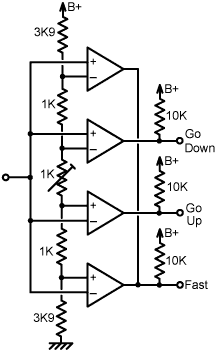
effects. The summing outputs in the circuits given above are shown feeding a window-comparator that produces two logic outputs "Go Down" ( |Z|>R0 ) and "Go Up" ( |Z|<R0 ). These may be fed to a microcontroller, or used to control an electric motor directly. The window adjustment sets a dead-band so that both outputs remain low while the bridge output stays within acceptable limits. Normal practice is to set the dead-band so that the tuning-cycle halts when load SWR falls below about 1.4 (this can be determined by reference to the carrier level, but an improved method is given in section 10). A somewhat tighter constraint is possible when an accurate bridge circuit is used, but note that it will not be possible to set a narrow window if there is residual RF in the input signal and the comparators are capable of responding to it. Additional low-pass filtering, such as a π-network (C-L-C), can be used between the summing network and the comparators if there is a problem. |
|
As alluded to above in the discussion
about time-constants, an automatic impedance-matching system
should be designed to work rapidly. Consequently, when electric
motors are used, there is danger of overshoot. The comparator
circuit on the right helps to get-around this problem by producing
an additional speed-switching logic signal, which is high when
the DC balance-error signal from the bridge is large. This can
be used to reduce the motor power-supply voltage as the matching-point
is approached. If open-collector comparators are used, the outputs
of the two extra comparators can be OR-connected (i.e., strapped
together). Note that if the motor drive circuitry of a permanent-magnet DC motor can sink current as well as source it, it will provide electrical braking when the motor needs to be slowed or stopped. |
 |
|
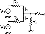
9. Summing-networks: We can prove that the simple resistor summing network produces a true arithmetical sum of voltages by analysing the circuit shown below. Here we have two DC generators with identical source resistances producing a voltage Vout across a load resistance Rp. Vout is given by: |
|
Vout = (I1 + I2) Rp where: I1 = (V1 - Vout) / Rs and I2 = (V2 - Vout) / Rs |
 |
|
Hence: Vout = (V1 - Vout + V2 - Vout) Rp / Rs i.e.: Vout = (V1 + V2 - 2Vout) Rp / Rs Adding 2VoutRp/Rs to each side gives: Vout (1 + 2 Rp / Rs) = (V1 + V2) Rp / Rs i.e.: Vout = (V1 + V2) Rp / [ Rs (1 + 2 Rp / Rs) ] and multiplying-out the denominator gives:
Hence the output is proportional to the sum of the two voltages and fulfils the requirements of an analog arithmetical adder. If we want to make a subtracter, all we have to do is reverse the connections to one of the generators. If we reverse the polarity of (say) the generator producing V2, then V2 changes sign in the equation above, and the output is proportional to the difference between the two voltages. Now notice what happens in the limit that R→∞. In that case, the 2Rp term overwhelms the denominator of equation (9.1) allowing Rs to be neglected. This gives: Vout = (V1 + V2) / 2 When a resistance is connected between the live terminals of two generators, the voltage at the centre-tap is equal to the true average of the two voltages. This is, of course, obvious; except perhaps for the caveat: the statement is only true when the generators are capable of sinking current as well as sourcing it. Diodes complicate matters; and if we wish to make absolute measurements of magnitude (such as for the purpose of evaluating bridge performance, to be discussed shortly) the refusal to pass reverse-current must be taken into account. |
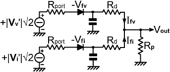
| The DC model for the difference circuit used in the instrumentation examples of the previous section is given below. Here we look back into the ports and see DC voltages of +|Vv'|√2 and -|Vi'|√2 by the action of ideal rectification; one of the notional generators being reversed by the equivalent operation of reversing a diode. The RF voltages are given primes because they are not identical to the off-load sample voltages; the reason being that the AC loading effect of the detector is not taken into account by the model. We expect however, by virtue of careful husbandry during the AC port-balancing phase of the design process, that the factor by which Vv' differs from Vv will be the same as the factor by which Vi' differs from Vi; and since the bridge is a linear network, this relationship will hold when the bridge is out of balance. Hence, AC loading does not affect the linearity of the summing process. |
|
The fact that the rectification
is not ideal is allowed-for by including the diode forward voltage
drops, so that the effective source voltages for insertion into
equation (9.1) above are: V1 = +(√2)|Vv'| - Vfv |
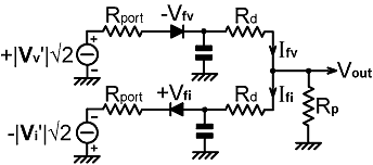 |
|
and V2 = -(√2)|Vi'| + Vfi Note however that the diode voltages are not fixed offsets, they are functions of the diode forward current (If) in the form: Vf = If Rds + mVT ln[( If / Is ) +1 ] where Rds is the diode series-resistance, m is an empirical parameter, VT=kT/q (=25.3mV at 20°C), and Is is the junction reverse-leakage current. [see: Diode detectors, diode correction function]. The IfRds term can be ignored if Rds is small relative to the other series resistances. Is and m will be the same for the two diodes if they are well matched, which they will be if two modern Schottky signal diodes (e.g., 1N5711) from the same manufacturing batch are used. What the diode equation tells us however, is that the two diode voltages will only be identical if the forward currents are the same. Hence they have each been given an extra subscript to distinguish them. The generator source resistances for comparison with equation (9.1) are both: Rs = Rport + Rd Rport is the DC resistance looking back into the port, and is the same for both generators by virtue of the DC port balancing phase of the design process. Rport can be practically zero if an RVS network with a compensating inductor is used. It can also be practically zero if an RF choke is placed across the port, but it is not usual to mention such practices in polite company (an RF choke of several mH will be operating above its SRF when used at HF radio frequencies, and so the resulting shunt impedance is anybody's guess). Now using equation (9.1) we get: Vout = [ (√2)|Vv'| - Vfv + -( √2)|Vi'| + Vfi ] Rp / (Rport + Rd + 2Rp ) The subtraction process is imperfect because of the term Vfi-Vfv , which although usually small, represents a deviation from linearity. Note however, what happens when we allow Rp to become very large. In that case, Ifv is forced to be the same as Ifi and so the non-linearity term disappears. Hence, as Rp→∞ we get: Vout = [ (√2)|Vv'| -( √2)|Vi'| ] / 2 i.e., since a number is the square of its own square-root: Vout = [ |Vv'| - |Vi'| ] / √2 The network becomes a perfect difference-engine when the output is unloaded. It is so by virtue of the fact that the diodes are connected anode to cathode, so that one generator always acts as a sink for current sourced by the other. We can make use of this property for the purpose of scientific measurement by dispensing with Rp and measuring the output with a high-input-resistance (i.e., electronic) voltmeter, or by connecting the output to the non-inverting input of an operational amplifier. The network is also a very good difference-engine when the output is loaded however; provided that there is sufficient RF drive to turn the diodes on hard (which by the logarithmic nature of the diode equation, minimises Vfi-Vfv). For many purposes (such as automatic impedance matching), perfect linearity is not important and, as mentioned previously, a finite value for Rd improves the system settling time. |
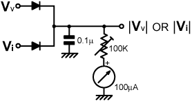
| A rather different situation prevails when the diodes are connected anode to anode, or cathode to cathode. In fact, the behaviour of the network is so complicated that we will be hard pressed to write a mathematical expression for it. |
| In the circuit shown on the right, the output will be approximately proportional to |Vv'|+|Vi'| when Rp is much smaller than Rport+Rd, but when Rp is large, the detector giving the highest voltage will turn-off the detector giving the lowest voltage, and the output will be proportional to a quasi-Boolean quantity |Vv| OR |Vi|. |
 |
| It is, of course, legitimate to ask why we should want to make magnitude summing bridges; but in fact, the information that can be obtained by this means has numerous uses. In the days before the invention of the reflectometer bridge, it was observed that, for the purpose of fault-detection in radio installations using open-wire feedlines (i.e., in the presence of standing waves), it was necessary to measure both the antenna current and the antenna voltage and combine the results. The reason is that, if (say) only the voltage is monitored, then a fault in the antenna system might cause a voltage minimum to appear at the measuring point, and the transmitter might catch fire before anyone realises that anything is wrong. A voltage minimum however, always corresponds to a current maximum, and so a protection system using combined current and voltage samples can never be fooled. |
| A device that makes an OR comparison between the voltage and current samples is "Alexander's Energy Indicator" [ US Pat. # 2467648 , 1949]. Nowadays it can be used as an RF level indicator, or to derive a transmitter output control (ALC) signal, which will remain valid in the presence of severe load mismatch. The circuit however, gives a flawed measurement of RF level, because its output when situated at a voltage maximum or a current maximum will be about twice its output when situated halfway between the maxima. A meaningful and more useful quantity is obtained by taking the true sum. |
 Alexander's Energy Indicator. |
|
Recall that, in reflectometry,
the quantity |Vv+Vi| (the output of a reversed impedance bridge)
is proportional to the square root of the forward power in a
transmission line. A magnitude summing bridge produces the quantity
|Vv|+|Vi|,
which is the same as |Vv+Vi| when the line is matched (Z=R0), but is always larger than |Vv+Vi| when the
line is mismatched. Hence |Vv|+|Vi| is a good ALC criterion that does not diminish
(i.e., request more power from the transmitter) when the line
is mismatched; and that is proportional to the square root of
the power delivered to a matched load. It was noted above, that when the DC sources cannot sink current, the accuracy of the sum produced by a resistive network increases as the resistance shunting the output is reduced. In fact, the output is true when the shunt resistance is zero; a situation that is not as useless as it might seem because we can feed the detector outputs into the virtual earth at the inverting input of an operational amplifier. Hence the circuit shown below is a true summing network, except that it has no compensation for detector non-linearity. |
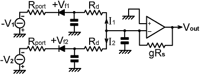 |
Summing network without diode compensation. When Rs=Rport+Rd, g is the DC voltage gain. |
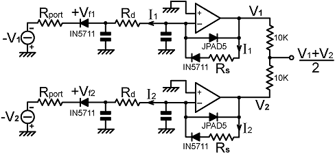
| In order to compensate for the diode forward voltage drop, the two detector outputs can, of course, be linearised before summing takes place. The circuit shown below uses a diode compensation method described in [Diode detectors, non-linearity correction], and achieves best accuracy when Rs=Rport+Rd. In practice, the operational amplifiers will usually require offset-nulling circuits, which are not shown. |
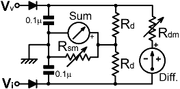
| Below right is a simple passive indicator that shows both the sum and the difference of the bridge-output magnitudes. It is most accurate when the resistance of the 'sum' meter (including its shunt) is low in comparison to Rd, and resistance of the 'difference' meter (including its series resistance) is high in comparison to Rd. |
| When the sensitivity of the difference meter is turned-up (Rdm is small), the sum meter turns into Alexander's Energy Indicator (it displays |Vv| OR |Vi| ). When the sensitivity of the sum meter is turned-up (Rsm is large), the sensitivity of the difference meter is reduced. The difference reading is in any case imperfect, because the detector giving the highest output will tend to turn-off the detector giving the lowest output (i,e, it displays |Vv| OR -|Vi| ); but it is acceptable for match-meters. |
 |
| If a passive arithmetical summing engine of reasonable accuracy is required, it can be made (albeit without detector non-linearity compensation) by stacking the outputs of the voltage and current sampling networks, as shown on the right. |
 |
| 9a. Logarithmic meter response: |
| Nulling instruments that rely on the use of a sensitivity control have a habit of wrapping the meter needle around the end-stop at the slightest provocation. This is particularly the case when the detector giving the highest output is able to turn-off its opponent; the 'OR' effect giving rise to something approximating an anti-logarithmic response. Such fierce behaviour can be prevented (and the need for a user sensitivity control can be eliminated) by adopting the simple circuit shown on the right. |
 |
|
The design approach for this diode-limiter
arrangement is most easily explained by using an example: A nulling
bridge, for insertion into a transmission-line, is designed so
that its two detectors are each giving just over +10V DC when
a radio transmitter is delivering its full output into a matched
load. The transmitter protection circuitry is adjusted so that
the transmitter can deliver either its maximum output voltage
or its maximum output current (but not both) when the the load
is severely mismatched. Hence the worst case for the indicating
meter is that one of the detectors will be producing +10V while
the other gives no output. If a 50-0-50 μA centre-zero meter is strapped between the two detectors, and both detectors are loaded with 10 kΩ resistors, the meter will be required to pass about 1 mA in the worst case (a factor of 20 overload). If a pair of diodes is connected between the two detector outputs (in parallel, anode to cathode), the maximum voltage difference will be limited to the diode forward voltage drop, which is given by the expression: Vf = Id Rds + mVT ln( 1 + Id / Is ) Rds is the diode series-resistance, m is an empirical parameter, VT=kT/q (=25.3mV at 20°C), and Is is the junction reverse-leakage current. [see Diode detectors, Diode correction func.]. Now, buy adjusting the total meter series resistance (Rm), it is possible to arrange things so that the meter has practically its full sensitivity for small differences in the detector outputs, but will only just touch the end-stop in the worst case. There is no analytical solution for Rm, but it is a straightforward matter to simulate the circuit and adjust for the desired outcome. Such a simulation is shown below, for a meter shunted by a pair of 1N5711 Schottky diodes (see spreadsheet: log_meter.ods ). |
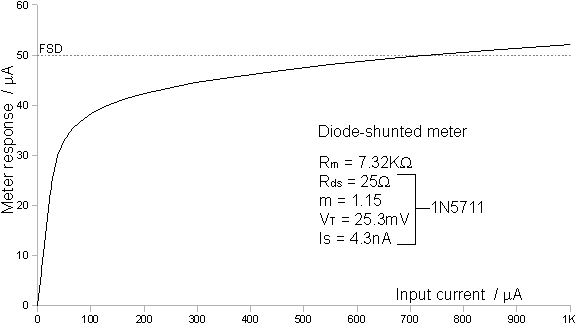
|
In this example, the meter series-resistance has been adjusted
to give 5% greater than full-scale deflection when the total
current (It) is 1mA. Rm
turns out to be 7.32 kΩ for this setting. Since typical
50-0-50 μA meters have internal resistance of around 1 kΩ,
the circuit is realisable in practice. Had we been using a somewhat
less sensitive meter, it might have been necessary to try diodes
having a larger forward voltage drop, such as the Silicon P-N
junction type 1N4148. Note that the best limiting action is obtained
with diodes having low internal resistance (Rds),
and the two diodes need to be reasonably well matched (Germanium
point-contact diodes are not good enough). In practice, meter adjustment is accomplished, not by torturing the radio transmitter, but by alternately disconnecting or shorting-out the RF drive to each of the detectors. Good diode matching ensures that maximum deflection is just coincident with the end-stop in both positive and negative directions. The use of diode limiting in order to obtain a roughly logarithmic meter response gives an enormous ergonomic improvement in nulling instruments. The point is that the meter always remains on-scale in normal use, and the sensitivity increases dramatically as the null is approached. The circuit is however unsuitable for the accurate measurement of bridge imbalance; because strapping the two detector outputs together (all bar a few hundred millivolts) exacerbates the OR effect. The tendency of one detector to turn-off the other can be ameliorated by placing a resistor in series with the meter network; but an accurate logarithmic response will not be achieved without reducing the sensitivity considerably. Also, the forward voltage of the limiter diodes is proportional to the absolute temperature, which means that only a crude calibration is possible. One caveat relating to the use of diode limiting in null indicators is that the instrument is always at maximum sensitivity in the region of the null. Hence it is essential to ensure that the nulling condition does not vary with drive-level; i.e., a logarithmic meter response will draw attention to any inadequacies in the port-balancing arrangements. |
|
10. Absolute measurements. For manual impedance matching applications, it is not necessary to have an exact knowledge of the load magnitude (or 'attribute of interest' in the general case). It is only necessary to know whether the attribute is too high or too low in comparison to the reference impedance (R0). For automatic systems however, it is essential to establish a termination criterion; i.e., an error window within which the impedance match can be said to be 'good enough'. For this we need some measure of the absolute error. We can also make use of the absolute error in the matter of evaluating a particular bridge, i.e., in finding out how good it is before adopting the circuit and putting it into service. In order to make an absolute measurement of impedance magnitude, all we have to do is take the ratio of the voltage and current sample magnitudes. This operation is somewhat analogous to the measurement of the reflection coefficient in a reflectometer bridge. The output of the current-sampling network of a current-transformer bridge (given earlier as equation 2.1) is: Vi = I Zi / N = V Zi / (N Z) After (ideal) rectification, we obtain a voltage proportional to |Vi|, where: |Vi| = |V| |Zi| / (N |Z| ) To compare this to the voltage sample; we note that all of the business of designing and calibrating the bridge is aimed at establishing a frequency-independent relationship such that: |Vv| = |Vi| when Z = R0 Hence: |Vv| = |V| |Zi| / (N R0) Hence, if we divide |Vv| by |Vi| we get:
Notice that the relationship above is dimensionless. It is true regardless of the absolute values of |Vv| and |Vi|, provided that the process by which the magnitudes were obtained (i.e., rectification) is linear. Notice also that, should both |Vv| and |Vi| change simultaneously (which, generally, they will when Z altered) we are at liberty, by virtue of only being interested in the ratio, to attribute the change entirely to one voltage or the other. Hence, if we decide to track the load magnitude by noting the change in |Vv| relative to |Vi|, we can write: |
|
|Vi| |
|
R0 |
|
i.e., if |Vv| =
|Vi| when |Z| = R0,
then:
By measuring the balance error in |Vv| as a proportion of |Vi|, we obtain the load impedance magnitude error as a proportion of R0. The simplest way in which to make use of the relationship above, is to adjust the generator output to achieve a pre-determined value of |Vi|; in which case, δ|Vv| is directly proportional to δ|Z|. We can make use of this information for the purpose of evaluating the bridge; using a simple perturbation method that relies on the fact that, if there is a difference between |Vv| and |Vi| when |Z| = R0 (due to a bridge error), then the balance error is negatively proportional to the impedance-magnitude error that will occur when the bridge is balanced; i.e., if the bridge is connected to a reference load (R0), then -δ|Vv| / |Vi| = δ|Z| / R0 where, in this case, δ|Z| represents the bridge accuracy at the test frequency. It is, of course, also possible on the basis of equation (10.3), to use |Vi| to control the output of a transmitter, so that δ|Vv| can be used directly as as criterion for turning an automatic impedance-matching system on or off. This is probably not a good idea however; firstly because it necessitates sending an ALC signal from the AMU to the transmitter, and secondly because transmitter internal protection circuits tend to override ALC signals. A far better approach is to use an analog ratio-computing engine, designed to work (within reason) regardless of carrier level. Then we can leave the transmitter to look-after itself, and the AMU control-systems become completely self-contained. |
|
10a. Analog ratio-computation methods: To the modern reader, perhaps the most obvious way in which to determine a ratio is to use a pair of analog-to-digital converters and a microcontroller. Analog computation methods have their merits however; particularly in producing signals that are directly usable by mechanical control systems, and that are well suited for display by that most highly-ergonomic of all electrical indicators; the moving-coil panel-meter. Standard analog computation practice is to represent numbers as voltages lying in the range -10 V to +10 V, using devices that work from a ±15 V power supply. A clean, fully-isolated and regulated ±15 V supply can be obtained from a 13.8 V source by means of a DC to DC converter module. Circuitry attendant upon a transmission-line bridge should take its ground reference from a single point on the transmission line; which means that any power lead should be fitted with one or more common-mode RF chokes. The circuits described below are not tried and tested construction projects. They are suggestions for practical investigation. Amplifier offset-nulling circuitry is not shown, and in some cases accuracy will be improved by including it. Four-quadrant multiplier. A four-quadrant multiplier is a device that, when presented with two input voltages VX and VY, produces an output proportional to VXVY. When working in the standard ±10 V analog computation space, it is usual for the output to be scaled by a factor of 1/10, so that when VX=±10 V and VY=±10 V, Vout=VXVY/10 = ±10 V. The adjective "four-quadrant" refers to the fact that the multiplier works for both positive and negative input values. The multiplier element is usually a circuit known as a 'Gilbert cell', which is a type of double-balanced mixer (DBM) that works accurately with both AC and DC signals. The Gilbert cell uses the logarithmic properties of bipolar transistors to perform an operation that corresponds to taking the logarithms of the two inputs, adding them together, and taking the anti-logarithm. The standard symbol for a mixer, being a multiplication symbol in a circle, reflects the fact that multiplication and mixing are one and the same (as does the habit of referring to a DBM as a "product detector"). Four-quadrant multipliers also usually have a summing input (Z), which can be used to shift the output level and also for various gain-control and feedback applications. An analog multiplier can compute squares (by joining the X and Y inputs together), and can compute square-roots and ratios when inserted into the feedback-loop of an operational amplifier. |
|
The Analog Devices
AD633 (scale-factor KS=10) is a low-cost
multiplier suitable for the applications under discussion here.
The ratio of two inputs can be obtained by inserting a multiplier into the feedback loop of an operational amplifier as shown below. |
|
Notice that the two resistors Re and Rf are connected to the virtual earth at the
input of an inverting amplifier. They must therefore inject equal
and opposite currents into the virtual earth. Hence: V2 / Re = - V1 Vout / (10 Rf) And so: Vout = -10 V2 Rf / (V1 Re) If we are representing numbers as voltages in the range -10 V to +10 V and the input voltages are positive, it makes sense to arrange matters so that Vout=-5 V when V1=V2. To do that, we choose Re=2Rf ; e.g., Re=20 kΩ and Rf=10 kΩ. Then to find the absolute difference between V2 and V1 as a proportion of V1 (such as for the purpose of computing magnitude error), we need to generate a voltage Vref=-10Rf/Re (i.e., -5 V probably) and compare it with Vout. One of the drawbacks with the circuit shown above is that the reference level has to be derived separately from the ratio-computing process. This means that the circuit is not self-adjusting, it will tend to drift, and any output error will be manifested in the all-important difference signal. The solution to this problem is to derive the reference voltage from the ratio-engine itself by using a commutator and a pair of sample-and-hold buffers. |
| Suitable switches, depending on the clocking arrangements, are the three-rail CMOS devices that operate from a ±15 V power-supply on the analog side but interface to standard digital logic (see, for example: DG411, 12, 13 and DG403). The clock signal should be a symmetric square-wave in the 500 Hz to 1 kHz range. Higher switching speeds are possible by using a more sophisticated clocking arrangement, particularly by allowing a settling-time between closing an input switch and sampling the output. It may also be desirable to stop the clock when the input voltages fall below a certain threshold (say 0.5 V), to prevent receiver interference. In that case, if both inputs are connected to V1, and the sample-hold switches are both on, both outputs will be forced to the reference level and the difference-signal will be zero (except for a few mV of offset-error). |
|
VCA: Another way of understanding the four-quadrant multiplier ratio-circuit is to see it as a voltage-controlled amplifier (VCA), with the gain controlled by the denominator input (V1). We can also make VCAs by using the voltage-controlled variable-resistance property of JFETs. A simple VCA with a very wide gain range can be made by putting a JFET in series with the input to an inverting operational amplifier. In this way, the virtual earth at the input provides a zero-reference for the FET source connection. |
|
In the circuit above, two VCAs are made to be as identical as
possible by using a dual N-channel JFET for the gain-controlling
elements. Suitable dual FETs are the venerable 2N3958 (now possibly obsolete) or its recommended
replacement the U3958.
The anti-latch-up diodes (gate to ground) are included within
the U3958 package and can be used by the simple expedient of
grounding the substrate pin. The gate resistor networks shown
give gate voltages from 0 to -5 V for a ±15 V output from
the control amplifier (the gate pinch-off voltage for the 2N/U3958
is guaranteed not to exceed -4.5 V). The control circuit computes the amount by which V1 must be amplified to make it equal to Vref. Hence: Vref = g V1 i.e.; g = Vref / V1 The gain-control voltage is applied to the other amplifier, setting its gain to g. Hence its output is V2Vref/V1. With the component values shown, the maximum gain of the VCAs is a little over -10. This allows the reference-voltage output to become stable when V1 is greater than about 0.5 V. The minimum gain can be arbitrarily small because the FET channels are effectively open-circuit at pinch-off, and so there is no upper limit on V1 and V2 save for the FET breakdown-voltage. If V1 and V2 are obtained from linear detectors based on op-amps, they can be made to go up to about +12.5 V, giving a 25:1 input voltage range (and a corresponding 625:1 transmitter power range). One possible drawback with the dual VCA circuit is that the gain laws of the two amplifiers might not be exactly identical. This will give rise to input-level-dependent zeroing errors (although they should not be serious, and offset-nulling circuits will help with the gain tracking for low input voltages). Also, it has to be said that dual matched JFETs can be rather expensive. Both of these problems can be solved by using a single VCA and a commutator. In this way, we can guarantee that both channels have exactly the same gain law, and only a single common-or-garden JFET is required. |
|
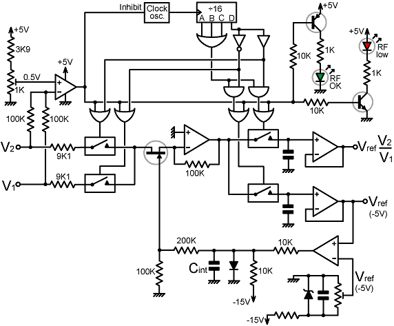
In the circuit above, all four CMOS switches are closed, and
the two outputs are forced to the same voltage, until the average
of V1 and V2 rises
above a preset threshold (shown as 0.5 V). When the threshold
is exceeded, the 'inhibit' line goes low, the clock oscillator
starts, and the switches are allowed to operate independently.
Switching waveforms are derived from the four outputs of a divide-by-16
counter (such as the 74HC93). The input switches operate alternately
for periods of 8 clock-cycles each. The output sample-and-hold
switches however, only close for 7 clock-periods, being forced
to miss the first period after the corresponding input switch
is closed. The minimum length of this waiting-period is, of course,
dictated by the amplifier settling-time. If we allow the amplifier
(say) 10 μs to settle, then the clock frequency is 100 kHz,
and the switching frequency is 100/16=6.25 kHz. The amplifier gain is controlled by comparing the reference output with a reference voltage, as in the dual VCA system. In this case however, the comparator output is a series of pulses that must be averaged to obtain the control voltage. This averaging is performed by the integration capacitor (Cint), which should be selected to give a critically-damped loop-response (i.e, just large enough to prevent overshoot when V1 undergoes a step change). |
|
|
|
|
|
|
|
|